


ADP1148, ADP1148-3.3, ADP1148-5
–4–
REV. A
CAUTION
ESD (electrostatic discharge) sensitive device. Electrostatic charges as high as 4000 V readily
accumulate on the human body and test equipment and can discharge without detection. Although
the ADP1148, ADP1148-3.3, ADP1148-5 feature proprietary ESD protection circuitry, permanent
damage may occur on devices subjected to high energy electrostatic discharges. Therefore, proper
ESD precautions are recommended to avoid performance degradation or loss of functionality.
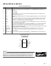
PIN FUNCTION DESCRIPTIONS
Pin # Mnemonic Function
1 P-Channel Drive High Current Gate Drive for Top P-Channel MOSFET. The voltage swing at Pin 4 is from V
IN
to
ground.
2 NC No Connection.
3V
IN
Input Voltage.
4C
T
External Capacitor C
T
from Pin 4 to Ground Sets the Operating Frequency. The frequency is also
dependent on the ratio V
OUT
/V
IN
.
5 Int V
CC
Internal Supply Voltage, Nominally 3.3 V. Must be decoupled to signal ground. Do not externally load
this pin.
6I
TH
Error Amplifier Decoupling Point. The current comparator threshold increases with the Pin 7 voltage.
7 Sense– Connects to internal resistive divider that sets the output voltage in ADP1148-3.3 and ADP1148-5
versions. Pin 7 is also the (–) input for the current comparator.
8 Sense+ The (+) Input for the Current Comparator. A built-in offset between Pins 7 and 8, in conjunction with
R
SENSE
, sets the current trip threshold.
9V
FB
For the ADP1148 adjustable version, Pin 9 serves as the feedback pin from an external resistive divider
used to set the output voltage. On ADP1148-3.3 and ADP1148-5 versions, this pin is not used.
10 Shutdown Taking Pin 10 of the ADP1148, ADP1148-3.3 or ADP1148-5 high holds both MOSFETs off. Must be
at ground potential for normal operation.
11 Signal GND Small Signal Ground. Must be routed separately from other grounds to the (–) terminal of C
OUT
.
12 Power GND Driver Power Ground. Connects to source of N-channel MOSFET and the (–) terminal of C
IN
.
13 NC No Connection.
14 N-Channel Drive High Current Drive for bottom N-channel MOSFET. The voltage swing at Pin 13 is from ground to
V
IN
.
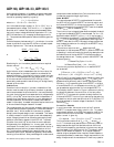
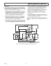
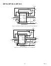
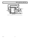
PIN CONFIGURATIONS
14-Lead Plastic DIP
14-Lead Plastic SO
14
13
12
11
10
9
8
1
2
3
4
7
6
5
TOP VIEW
(Not to Scale)
NC = NO CONNECT
P-DRIVE
SIGNAL GND
POWER GND
NC
N-DRIVE
NC
V
IN
C
T
ADP1148
SENSE(+)
V
FB
*
SHUTDOWN
INT V
CC
I
TH
SENSE(–)
*FIXED OUTPUT VERSIONS = SD1
WARNING!
ESD SENSITIVE DEVICE