


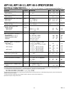


ADP1148, ADP1148-3.3, ADP1148-5
–11–
REV. A
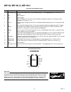
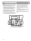
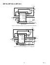
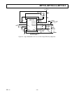
Board Layout
When laying out the printed circuit board, the following check
list should be used to ensure proper operation of the ADP1148.
These items are also illustrated graphically in the layout diagram
of Figure 18. Check the following in your layout:
1) Are the signal and power grounds segregated? The ADP1148
SIGNAL GND (Pin 11) must return to the (–) plate of C
OUT
.
The power ground returns to the source of the N-channel
MOSFET, anode of the Schottky diode, and (–) plate of C
IN
,
which should have as short lead lengths as possible.
2) Does the ADP1148 SENSE(–), (Pin 7), connect to a point
close to R
SENSE
and the (+) plate Of C
OUT
? In adjustable
versions the resistive divider R1, R2 must be connected be-
tween the (+) plate of C
OUT
and signal ground.
3) Are the SENSE(–) and SENSE(+) leads routed together with
minimum PC trace spacing? The 1000 pF capacitor between
Pins 7 and 8 should be as close as possible to the ADP1148.
4) Does the (+) plate of C
IN
connect to the source of the
P-channel MOSFET as closely as possible? This capacitor
provides the ac current to the P-channel MOSFET.
5) Is the input decoupling capacitor (1 µF) connected closely
between V
IN
(Pin 3) and POWER GND (Pin 12)? This
capacitor carries the MOSFET driver peak currents.
6) Is INTV
CC
(Pin 5) decoupled with a 10 nF capacitor to
signal ground?
7) Is the SHUTDOWN (Pin 10) actively pulled to ground
during normal operation? The Shutdown pin is high imped-
ance and must not be allowed to float.
To prevent noise spikes from erroneously tripping the current
comparator, a 1000 pF capacitor is needed across Sense(–) and
Sense(+).
P-DRIVE
NC
V
IN
C
T
INT V
CC
I
TH
SENSE(–)
N-DRIVE
NC
POWER GND
SIGNAL GND
SHUTDOWN
V
FB
SENSE(+)
ADP1148
3300pF
1k⍀
D1
C
IN
L
R1
R2
C
OUT
10nF
C
T
1F
1
2
3
4
5
6
7
14
13
12
11
10
9
8
N-CHANNEL
1000pF
R1, R2 OUTPUT DIVIDER REQUIRED
FOR ADJUSTABLE VERSION ONLY.
R
SENSE
–
–
V
IN
V
OUT
P-CHANNEL
NC = NO CONNECT
Figure 18. ADP1148 Layout Diagram (See Board Layout)