


SDAIBB1300 Manual 9
B&B Electronics Mfg Co Inc – 707 Dayton Rd - PO Box 1040 - Ottawa IL 61350 - Ph 815-433-5100 - Fax 815-433-5104
Chapter 3: Configuration
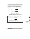
Output Offset
The output offset is the amount by which the output is shifted.
Equation 1 shows how the output offset affects the output of the buffer.
The negative output rail will clip any reading that has a negative input
differential unless the buffer’s output offset is raised. For this purpose,
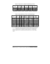
output offsets of 0 V and 2.5 V are individually jumper selectable for each
channel on the SDAIBB when mated with a compatible data acquisition
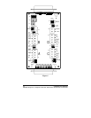
model. JP5 corresponds to channel A, JP6 corresponds with channel B,
JP7 corresponds with channel C, and JP8 corresponds with channel D.
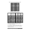
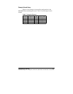
An output offset of 0 V is always available. See Table 4 for a list
of models that support the 2.5 V output offset. An output offset of 0 V is
used for positive only differentials, and an output offset of 2.5 V provides
the maximum input range for signals that run equally positive and negative.
A different output offset may be brought in on the terminal blocks
with the output offset jumper removed on the corresponding channel.
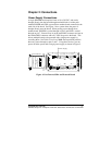
Gain Selection
The gain is individually selectable on each buffer with a two-
position jumper. Gains of 1 and 22.28 are conveniently provided on the
unit for each buffer. JP1 controls the gain on channel A, JP2 controls B,
JP3 controls C, and JP4 controls D. Unity gain is ideal for eliminating the
impedance mismatch between input devices and the data acquisition
module. Table 5 shows the maximum voltage ranges that can be amplified
by the provided gain of 22.28. To change the gain, leave the jumper in the
User/22.28 gain position, remove the through-hole 4.7 kΩ resistor, and
replace it with the appropriate value. See Table 6 for some standard inputs,
gains, and appropriate resistor values to achieve the expected gain.
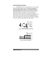
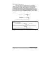
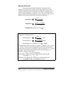
Equation 1:
()
etOutputOffsGainININV
out
+−=
−+