


10 SDAIBB1300 Manual
B&B Electronics Mfg Co Inc – 707 Dayton Rd - PO Box 1040 - Ottawa IL 61350 - Ph 815-433-5100 - Fax 815-433-5104
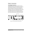
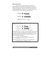
Change R1 to change the gain on channel A, R2 to change channel
B, R7 to change channel C, and R8 to change channel D. The following
sections explain how to calculate the gain and gain resistor for other input
ranges.
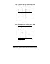
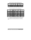
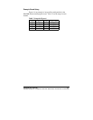
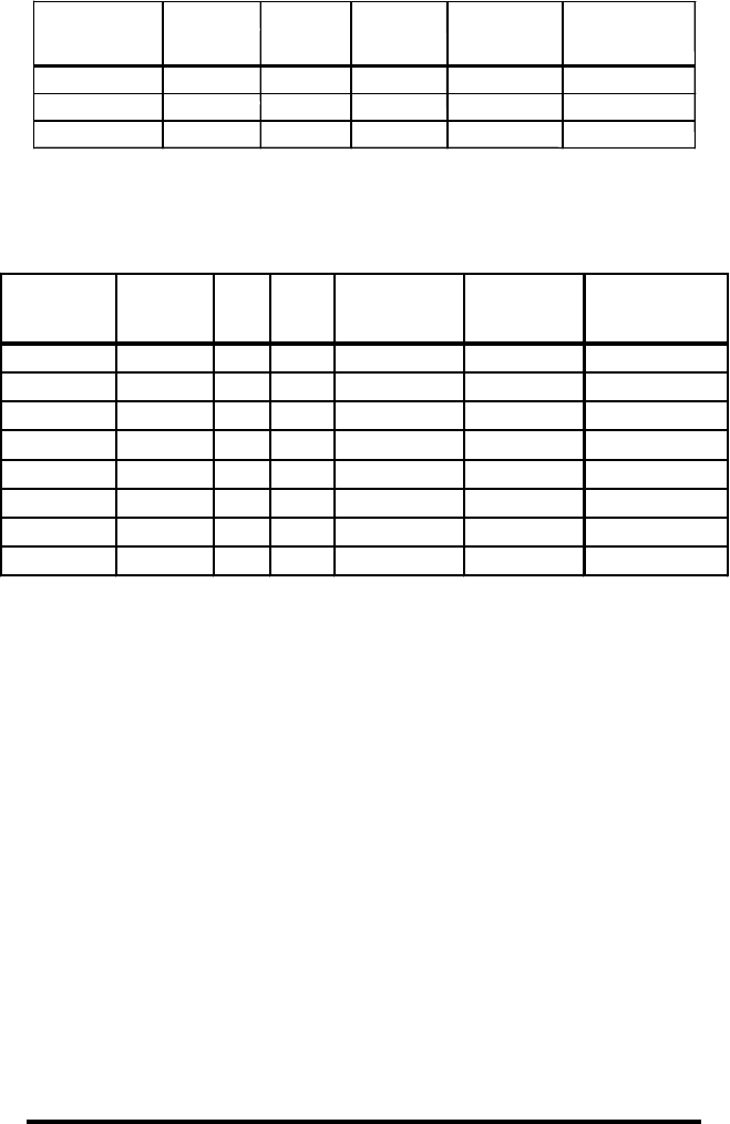
Table 5: Values for Use with the Provided Gain of 22.28
VCM VDIFF Out Ref
1%
Resistor
Calculated
Gain
Output
Range
27.5 mV max +55 mV 0 V 4.7 k
Ω
22.28 0.01 – 1.23 V
0 V ±52 mV 2.5 V 4.7 k
Ω
22.28 1.32 - 3.68 V
2.5 V ±110 mV 2.5 V 4.7 k
Ω
22.28 0.03 - 4.97 V
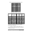
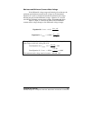
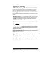
Table 6: Gains and Resistor Values for Standard Inputs
V
CM
V
DIFF
Out
Ref
G
MAX
Closest 1%
Resistor
Calculated
Gain
Output
Range
5mV max +10 mV 0V 119
866
Ω
116.47 0.01 - 1.16 V
50mV max +100mV 0V 12.8
8.66 k
Ω
12.55 0.01 - 1.25 V
0.5V max +1 V 0V 2.18
86.6 k
Ω
2.15 0.01 - 2.18 V
0V ±10 mV 2.5V 118
866
Ω
116.47 1.34 - 3.66 V
0V ±100 mV 2.5V 11.8
9.31 k
Ω
11.74 1.32 - 3.67 V
2.5V ±10 mV 2.5V 247
412
Ω
243.72 0.06 - 4.94 V
2.5V ±100 mV 2.5V 24.7
4.32 k
Ω
24.15 0.09 - 4.91 V
2.5V ±1 V 2.5V 2.47
69.8 k
Ω
2.43 0.07 - 4.93 V