


SDAIBB1300 Manual 5
B&B Electronics Mfg Co Inc – 707 Dayton Rd - PO Box 1040 - Ottawa IL 61350 - Ph 815-433-5100 - Fax 815-433-5104
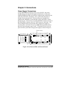
Input Voltage Connections
The SDAIBB can receive signals in the range of –0.15 to +5 VDC
when set to unity gain, and –0.15 to +3.5 VDC when set to any other gain.
Note: This voltage reading is taken from GND on the SDAIBB to
Input+ and GND to Input- voltages. It is
not
the differential voltage
from Input- to Input+.
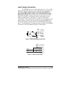
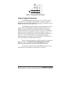
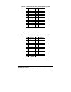
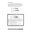
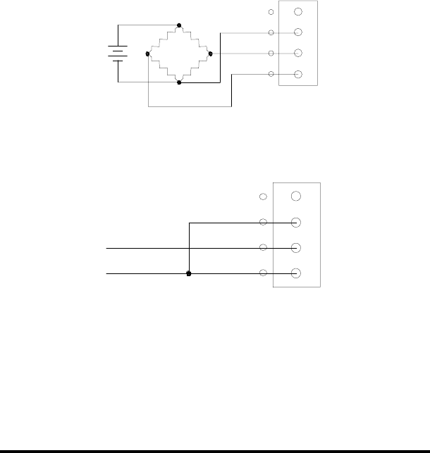
Signals are brought into the buffer by terminal
blocks or solder pads. The terminal blocks are labeled Input+, Input-,
GND, and Output Offset. See Figures 3, 4, and 5 for typical input
configurations. The voltage that will be amplified is the reading taken from
Input- to Input+. GND is connected to the ground of the SDAIBB and is
provided for making a common reference for the SDAIBB and the input
device. The Output Offset is an input that shifts the output of the SDAIBB.
This feature is discussed further in Chapter 3, Output Offset.
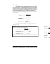
OUT
OFF
GND
IN+
IN-
Figure 3: Differential Signal with GND
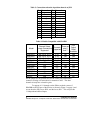
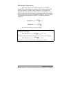
OUT
OFF
GND
IN+
IN-
Signal
GND
Figure 4: Single Ended Signal