6 SDAIBB1300 Manual
B&B Electronics Mfg Co Inc – 707 Dayton Rd - PO Box 1040 - Ottawa IL 61350 - Ph 815-433-5100 - Fax 815-433-5104
Output Voltage Connections
The SDAIBB outputs voltages from +0.1 to +5.0 VDC at unity
gain, and +0.1 to +4.95 VDC at any other gain. All lines are carried
straight through on the DB25 connectors, allowing for the addition of extra
channels by connecting on another board.
The SDAIBB output connections are jumper selectable to line up
with the channels of the B&B line of SDAxx data acquisition devices.
When the 4-position shunt is set to JP9, input buffer A is connected to
channel 0 on pin 8, B is connected to channel 1 on pin 9, C is connected to
channel 2 on pin 10, and buffer D is connected to channel 3 on pin 11.
Setting the 4-position shunt to JP10 connects the buffers to channels 4 to 7
(pins 12, 13, 21, and 22 respectively), and setting the shunt to JP11
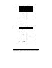
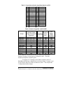
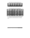
connects the buffers to channels 8 to 10 (pins 23 to 25). See Table 1 for a
list of the connections when the jumper is on JP9,
Table 2 for when the jumper is on JP10, and Table 3 for when the
jumper is on JP11.
Note: When the 4-position jumper is on JP11,
buffer D is not connected to any pins on the DB25 connector.
For a listing of which modules the SDAIBB can connect to and
which channels are compatible on each module, see Table 4.
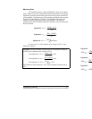
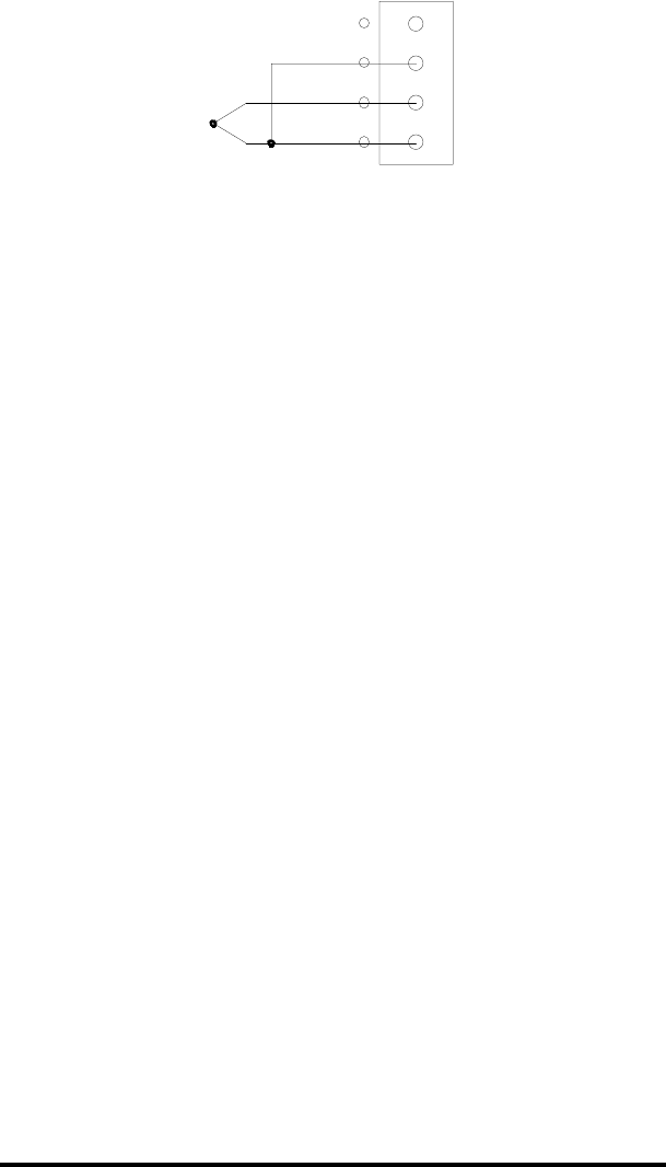
OUT
OFF
GND
IN+
IN-
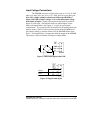
Figure 5: Floating Differential Signal


