


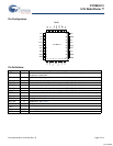


CY7B9911V
3.3V RoboClock+™
Document Number: 38-07408 Rev. *D Page 3 of 14
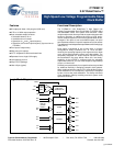
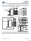
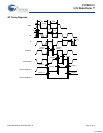
Block Diagram Description
Phase Frequency Detector and Filter
The Phase Frequency Detector and Filter blocks accept inputs
from the Reference Frequency (REF) input and the Feedback
(FB) input. They generate correction information to control the
frequency of the Voltage Controlled Oscillator (VCO). These
blocks, along with the VCO, form a Phase Locked Loop (PLL)
that tracks the incoming REF signal.
VCO and Time Unit Generator
The VCO accepts analog control inputs from the PLL filter block.
It generates a frequency used by the time unit generator to
create discrete time units that are selected in the skew select
matrix. The operational range of the VCO is determined by the
FS control pin. The time unit (t
U
) is determined by the operating
frequency of the device and the level of the FS pin as shown in
Table 1.
Skew Select Matrix
The skew select matrix is comprised of four independent
sections. Each section has two low skew, high fanout drivers
(xQ0, xQ1), and two corresponding three level function select
(xF0, xF1) inputs. Table 2 shows the nine possible output
functions for each section as determined by the function select
inputs. All times are measured with respect to the REF input
assuming that the output connected to the FB input has 0t
U
selected.
Table 1. Frequency Range Select and t
U
Calculation
[1]
FS
[2, 3]
f
NOM
(MHz)
where N =
Approximate
Frequency (MHz) At
Which t
U
= 1.0 ns
Min Max
LOW 15 30 44 22.7
MID 25 50 26 38.5
HIGH 40 110 16 62.5
t
U
1
f
NOM
N×
------------------------
=
Table 2. Programmable Skew Configurations
[1]
Function Selects Output Functions
1F1, 2F1,
3F1, 4F1
1F0, 2F0,
3F0, 4F0
1Q0, 1Q1,
2Q0, 2Q1
3Q0, 3Q1 4Q0, 4Q1
LOW LOW –4t
U
Divide by 2 Divide by 2
LOW MID –3t
U
–6t
U
–6t
U
LOW HIGH –2t
U
–4t
U
–4t
U
MID LOW –1t
U
–2t
U
–2t
U
MID MID 0t
U
0t
U
0t
U
MID HIGH +1t
U
+2t
U
+2t
U
HIGH LOW +2t
U
+4t
U
+4t
U
HIGH MID +3t
U
+6t
U
+6t
U
HIGH HIGH +4t
U
Divide by 4 Inverted
Notes
1. For all three-state inputs, HIGH indicates a connection to V
CC
, LOW indicates a connection to GND, and MID indicates an open connection. Internal termination
circuitry holds an unconnected input to V
CC
/2.
2. The level to be set on FS is determined by the “normal” operating frequency (f
NOM
) of the V
CO
and Time Unit Generator (see). Nominal frequency (f
NOM
) always
appears at 1Q0 and the other outputs when they are operated in their undivided modes (see Tab le 2). The frequency appearing at the REF and FB inputs is f
NOM
when the output connected to FB is undivided. The frequency of the REF and FB inputs is f
NOM
/2 or f
NOM
/4 when the part is configured for a frequency multiplication
using a divided output as the FB input.
3. When the FS pin is selected HIGH, the REF input must not transition upon power up until V
CC
has reached 2.8V.
[+] Feedback