


CY7B9911V
3.3V RoboClock+™
Document Number: 38-07408 Rev. *D Page 7 of 14
frequency, while still maintaining the low skew characteristics of
the clock driver. The LVPSCB performs all of the functions
described in this section at the same time. It can multiply by two
and four or divide by two (and four) at the same time. This shifts
its outputs over a wide range or maintain zero skew between
selected outputs.
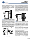
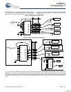
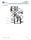
Figure 8 shows the CY7B9911V connected in series to construct a zero skew clock distribution tree between boards. Delays of the
downstream clock buffers are programmed to compensate for the wire length (that is, select negative skew equal to the wire delay)
necessary to connect them to the master clock source, approximating a zero delay clock tree. Cascaded clock buffers accumulates
low frequency jitter because of the non-ideal filtering characteristics of the PLL filter. Do not connect more than two clock buffers in a
series.
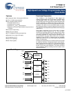
Figure 7. Multi-Function Clock Driver
Figure 8. Board-to-Board Clock Distribution
27.5 MHz
DISTRIBUTION
CLOCK
110 MHz
INVERTED
Z
0
27.5 MHz
110 MHz
ZERO SKEW
110 MHz
SKEWED –2.273 ns (–4t
U
)
FB
REF
FS
4F0
4F1
3F0
3F1
2F0
2F1
1F0
1F1
4Q0
4Q1
3Q0
3Q1
2Q0
2Q1
1Q0
1Q1
TEST
REF
LOAD
LOAD
LOAD
LOAD
Z
0
Z
0
Z
0
SYSTEM
CLOCK
Z
0
L1
L2
L3
L4
FB
REF
FS
4F0
4F1
3F0
3F1
2F0
2F1
1F0
1F1
4Q0
4Q1
3Q0
3Q1
2Q0
2Q1
1Q0
1Q1
TEST
REF
4F0
4F1
3F0
3F1
2F0
2F1
1F0
1F1
4Q0
4Q1
3Q0
3Q1
2Q0
2Q1
1Q0
1Q1
REF
FS
FB
LOAD
LOAD
LOAD
LOAD
LOAD
TEST
Z
0
Z
0
Z
0
[+] Feedback