


CY7B9911V
3.3V RoboClock+™
Document Number: 38-07408 Rev. *D Page 5 of 14
Operational Mode Descriptions
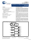
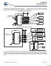
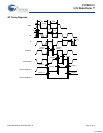
Figure 2 shows the LVPSCB configured as a zero skew clock buffer. In this mode the CY7B9911V is used as the basis for a low skew
clock distribution tree. When all the function select inputs (xF0, xF1) are left open, each of the outputs are aligned and drive a
terminated transmission line to an independent load. The FB input is tied to any output in this configuration and the operating frequency
range is selected with the FS pin. The low skew specification, along with the ability to drive terminated transmission lines (with
impedances as low as 50Ω), enables efficient printed circuit board design.
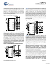
Figure 3 shows a configuration to equalize skew between metal
traces of different lengths. In addition to low skew between
outputs, the LVPSCB is programmed to stagger the timing of its
outputs. Each of the four groups of output pairs is programmed
to different output timing. Skew timing is adjusted over a wide
range in small increments with the appropriate strapping of the
function select pins. In this configuration the 4Q0 output is sent
back to FB and configured for zero skew. The other three pairs
of outputs are programmed to yield different skews relative to the
feedback. By advancing the clock signal on the longer traces or
retarding the clock signal on shorter traces, all loads receive the
clock pulse at the same time.
In Figure 3 the FB input is connected to an output with 0 ns skew
(xF1, xF0 = MID) selected. The internal PLL synchronizes the FB
and REF inputs and aligns their rising edges to make certain that
all outputs have precise phase alignment.
Clock skews are advanced by ±6 time units (tU) when using an
output selected for zero skew as the feedback. A wider range of
delays is possible if the output connected to FB is also skewed.
Since “Zero Skew”, +tU, and –tU are defined relative to output
Figure 2. Zero Skew and Zero Delay Clock Driver
SYSTEM
CLOCK
L1
L2
L3
L4
LENGTH L1 = L2 = L3 = L4
FB
REF
FS
4F0
4F1
3F0
3F1
2F0
2F1
1F0
1F1
4Q0
4Q1
3Q0
3Q1
2Q0
2Q1
1Q0
1Q1
TEST
Z
0
LOAD
LOAD
LOAD
LOAD
REF
Z
0
Z
0
Z
0
Figure 3. Programmable Skew Clock Driver
LENGTH L1 = L2
L3 < L2 by 6 inches
L4 > L2 by 6 inches
SYSTEM
CLOCK
L1
L2
L3
L4
FB
REF
FS
4F0
4F1
3F0
3F1
2F0
2F1
1F0
1F1
4Q0
4Q1
3Q0
3Q1
2Q0
2Q1
1Q0
1Q1
TEST
Z
0
LOAD
LOAD
LOAD
LOAD
REF
Z
0
Z
0
Z
0
[+] Feedback