


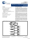


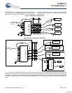
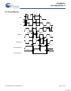


CY7B9911V
3.3V RoboClock+™
Document Number: 38-07408 Rev. *D Page 8 of 14
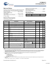
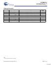
Maximum Ratings
Operating outside these boundaries may affect the performance
and life of the device. These user guidelines are not tested.
Storage Temperature ................................. –65°C to +150°C
Ambient Temperature with
Power Applied ............................................ –55°C to +125°C
Supply Voltage to Ground Potential................–0.5V to +7.0V
DC Input Voltage ............................................–0.5V to +7.0V
Output Current into Outputs (LOW)............................. 64 mA
Static Discharge Voltage...........................................> 2001V
(MIL-STD-883, Method 3015)
Latch up Current.....................................................> 200 mA
Operating Range
Range Ambient Temperature V
CC
Commercial 0°C to +70°C 3.3V ± 10%
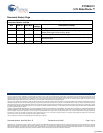
Electrical Characteristics
Over the Operating Range
[5]
Parameter Description Test Conditions
CY7B9911V
Unit
Min Max
V
OH
Output HIGH Voltage V
CC
= Min, I
OH
= –18 mA 2.4 V
V
OL
Output LOW Voltage V
CC
= Min, I
OL
= 35 mA 0.45 V
V
IH
Input HIGH Voltage (REF and FB inputs only) 2.0 V
CC
V
V
IL
Input LOW Voltage (REF and FB inputs only) –0.5 0.8 V
V
IHH
Three Level Input HIGH Voltage (Test, FS,
xFn)
[5]
Min ≤ V
CC
≤ Max 0.87 * V
CC
V
CC
V
V
IMM
Three Level Input MID Voltage (Test, FS,
xFn)
[5]
Min ≤ V
CC
≤ Max 0.47 * V
CC
0.53 * V
CC
V
V
ILL
Three Level Input LOW Voltage (Test, FS,
xFn)
[5]
Min ≤ V
CC
≤ Max 0.0 0.13 * V
CC
V
I
IH
Input HIGH Leakage Current (REF and FB
inputs only)
V
CC
= Max, V
IN
= Max 20 μA
I
IL
Input LOW Leakage Current (REF and FB
inputs only)
V
CC
= Max, V
IN
= 0.4V –20 μA
I
IHH
Input HIGH Current (Test, FS, xFn) V
IN
= V
CC
200 μA
I
IMM
Input MID Current (Test, FS, xFn) V
IN
= V
CC
/2 –50 50 μA
I
ILL
Input LOW Current (Test, FS, xFn) V
IN
= GND –200 μA
I
OS
Short Circuit Current
[7]
V
CC
= MAX, V
OUT
= GND (25° only) –200 mA
I
CCQ
Operating Current Used by Internal Circuitry V
CCN
= V
CCQ
= Max, All
Input Selects Open
Com’l 95 mA
Mil/Ind 100
I
CCN
Output Buffer Current per Output Pair
[8]
V
CCN
= V
CCQ
= Max,
I
OUT
= 0 mA Input Selects Open, f
MAX
19 mA
PD Power Dissipation per Output Pair
[9]
V
CCN
= V
CCQ
= Max,
I
OUT
= 0 mA Input Selects Open, f
MAX
104 mW
Notes
5. For more information see Group A subgroup testing information
.
6. These inputs are normally wired to VCC, GND, or left unconnected (actual threshold voltages vary as a percentage of VCC). Internal termination resistors hold
unconnected inputs at VCC/2. If these inputs are switched, the function and timing of the outputs glitch and the PLL may require an additional tLOCK time
before all data sheet limits are achieved.
7. CY7B9911V must be tested one output at a time, output shorted for less than one second, less than 10% duty cycle. Room temperature only.
8. Total output current per output pair is approximated by the following expression that includes device current plus load current:
CY7B9911V:ICCN = [(4 + 0.11F) + [[((835 –3F)/Z) + (.0022FC)]N] x 1.1
Where
F = frequency in MHz
C = capacitive load in pF
Z = line impedance in ohms
N = number of loaded outputs; 0, 1, or 2
FC = F < C
9. Total power dissipation per output pair is approximated by the following expression that includes device power dissipation plus power dissipation due to the
load circuit:
PD = [(22 + 0.61F) + [[(1550 + 2.7F)/Z) + (.0125FC)]N] x 1.1. (See note 8 for variable definition.)
[+] Feedback