


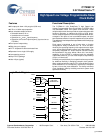
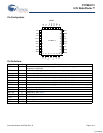


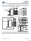


CY7B9911V
3.3V RoboClock+™
Document Number: 38-07408 Rev. *D Page 9 of 14
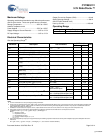
Capacitance
Tested initially and after any design or process changes that may affect these parameters.
[10]
Parameter Description Test Conditions Max Unit
C
IN
Input Capacitance T
A
= 25°C, f = 1 MHz, V
CC
= 3.3V 10 pF
Note
10.Applies to REF and FB inputs only.
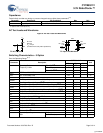
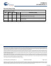
AC Test Loads and Waveforms
Switching Characteristics – 5 Option
Over the Operating Range
[2, 11]
Parameter Description
CY7B9911V-5
Unit
Min Typ Max
f
NOM
Operating Clock
Frequency in MHz
FS = LOW
[1, 2]
15 30 MHz
FS = MID
[1, 2]
25 50
FS = HIGH
[1, 2 , 3]
40 110
t
RPWH
REF Pulse Width HIGH 5.0 ns
t
RPWL
REF Pulse Width LOW 5.0 ns
t
U
Programmable Skew Unit See Table 1
t
SKEWPR
Zero Output Matched-Pair Skew (XQ0, XQ1)
[13, 14]
0.1 0.25 ns
t
SKEW0
Zero Output Skew (All Outputs)
[13, 15]
0.25 0.5 ns
t
SKEW1
Output Skew (Rise-Rise, Fall-Fall, Same Class Outputs)
[13, 17]
0.6 0.7 ns
t
SKEW2
Output Skew (Rise-Fall, Nominal-Inverted, Divided-Divided)
[13, 17]
0.5 1.0 ns
t
SKEW3
Output Skew (Rise-Rise, Fall-Fall, Different Class Outputs)
[17, 17]
0.5 0.7 ns
t
SKEW4
Output Skew (Rise-Fall, Nominal-Divided, Divided-Inverted)
[13, 17]
0.5 1.0 ns
t
DEV
Device-to-Device Skew
[12, 18]
1.25 ns
t
PD
Propagation Delay, REF Rise to FB Rise –0.5 0.0 +0.5 ns
t
ODCV
Output Duty Cycle Variation
[19]
–1.0 0.0 +1.0 ns
t
PWH
Output HIGH Time Deviation from 50%
[20]
2.5 ns
t
PWL
Output LOW Time Deviation from 50%
[20]
3ns
t
ORISE
Output Rise Time
[20, 21]
0.15 1.0 1.5 ns
t
OFALL
Output Fall Time
[20, 21]
0.15 1.0 1.5 ns
t
LOCK
PLL Lock Time
[22]
0.5 ms
t
JR
Cycle-to-Cycle Output
Jitter
RMS
[12]
25 ps
Peak-to-Peak
[12]
200 ps
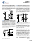
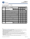
TTL ACTest Load TTL Input Test Waveform
V
CC
R1
R2
C
L
3.0V
2.0V
V
th
=1.5V
0.8V
0.0V
≤1ns
≤1ns
2.0V
0.8V
V
th
=1.5V
R1=100
R2=100
C
L
=30pF
(Includes fixture and probe capacitance)
Figure 9. AC Test Loads and Waveforms
[+] Feedback