


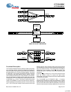
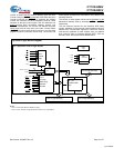
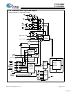
CY7C0430BV
CY7C0430CV
Document #: 38-06027 Rev. *B Page 10 of 37
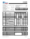
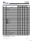
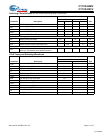
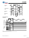
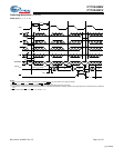
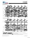
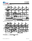
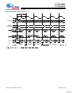
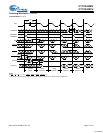
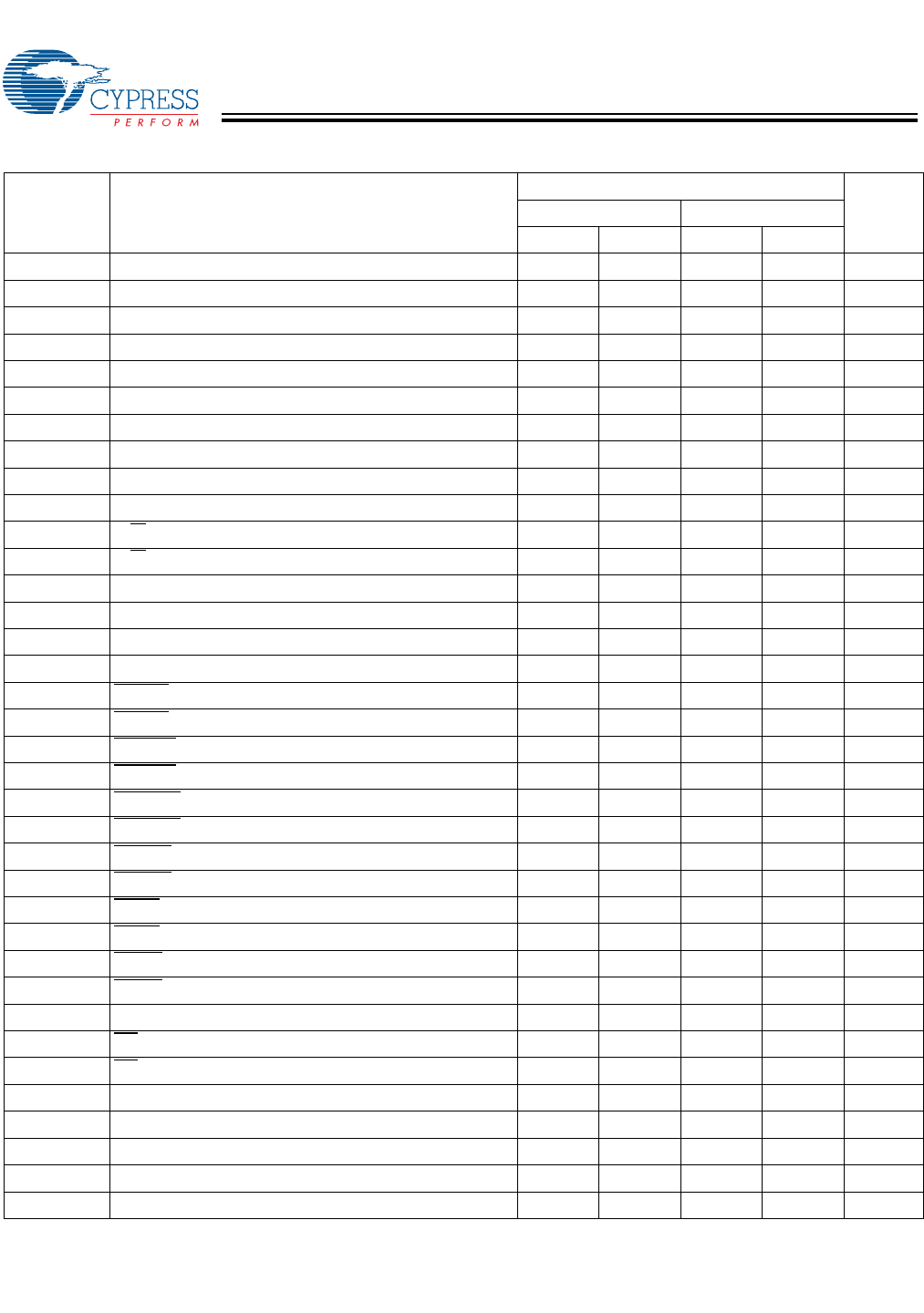
Switching Characteristics Over the Industrial Operating Range
[6]
Parameter Description
CY7C0430BV and CY7C0430CV
Unit
–133 –100
Min. Max. Min. Max.
f
MAX2
[7]
Maximum Frequency 133 100 MHz
t
CYC2
[7]
Clock Cycle Time 7.5 10 ns
t
CH2
Clock HIGH Time 3 4 ns
t
CL2
Clock LOW Time 3 4 ns
t
R
Clock Rise Time 2 3 ns
t
F
Clock Fall Time 2 3 ns
t
SA
Address Set-up Time 2.3 3 ns
t
HA
Address Hold Time 0.7 0.7 ns
t
SC
Chip Enable Set-up Time 2.3 3 ns
t
HC
Chip Enable Hold Time 0.7 0.7 ns
t
SW
R/W Set-up Time 2.3 3 ns
t
HW
R/W Hold Time 0.7 0.7 ns
t
SD
Input Data Set-up Time 2.3 3 ns
t
HD
Input Data Hold Time 0.7 0.7 ns
t
SB
Byte Set-up Time 2.3 3 ns
t
HB
Byte Hold Time 0.7 0.7 ns
t
SCLD
CNTLD Set-up Time 2.3 3 ns
t
HCLD
CNTLD Hold Time 0.7 0.7 ns
t
SCINC
CNTINC Set-up Time 2.3 3 ns
t
HCINC
CNTINC Hold Time 0.7 0.7 ns
t
SCRST
CNTRST Set-up Time 2.3 3 ns
t
HCRST
CNTRST Hold Time 0.7 0.7 ns
t
SCRD
CNTRD Set-up Time 2.3 3 ns
t
HCRD
CNTRD Hold Time 0.7 0.7 ns
t
SMLD
MKLD Set-up Time 2.3 3 ns
t
HMLD
MKLD Hold Time 0.7 0.7 ns
t
SMRD
MKRD Set-up Time 2.3 3 ns
t
HMRD
MKRD Hold Time 0.7 0.7 ns
t
OE
Output Enable to Data Valid 6.5 8 ns
t
OLZ
[8]
OE to Low-Z 1 1 ns
t
OHZ
[8]
OE to High-Z 1 6 1 7 ns
t
CD2
Clock to Data Valid 4.2 5 ns
t
CA2
Clock to Counter Address Readback Valid 4.7 5 ns
t
CM2
Clock to Mask Register Readback Valid 4.7 5 ns
t
DC
Data Output Hold After Clock HIGH 1 1 ns
t
CKHZ
[9]
Clock HIGH to Output High-Z 1 4.8 1 6.8 ns
Notes:
6. If data is simultaneously written and read to the same address location and t
CCS
is violated, the data read from the address, as well as the subsequent data
remaining in the address is undefined.
7. f
MAX2
for commercial is 135 MHz. t
CYC2
Min. for commercial is 7.4 ns.
8. This parameter is guaranteed by design, but it is not production tested.
9. Valid for both address and data outputs.
[+] Feedback