


CY7C0430BV
CY7C0430CV
Document #: 38-06027 Rev. *B Page 14 of 37
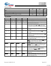
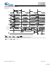
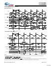
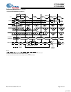
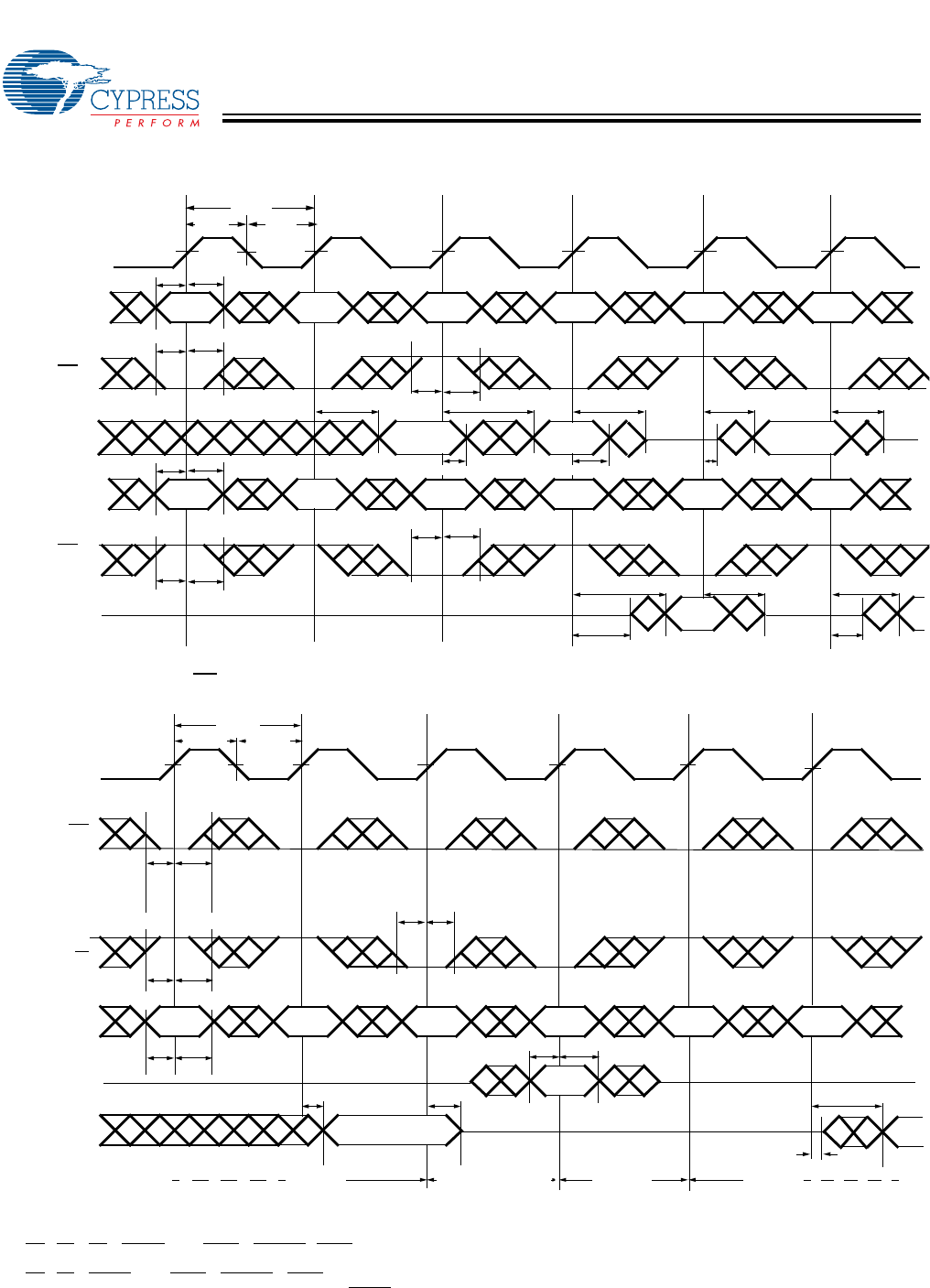
Bank Select Read
[17, 18]
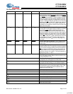
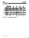
Read-to-Write-to-Read (OE = V
IL
)
[19, 20, 21, 22]
Notes:
17.In this depth expansion example, B1 represents Bank #1 and B2 is Bank #2; Each bank consists of one QuadPort DSE device from this data sheet.
ADDRESS
(B1)
= ADDRESS
(B2)
.
18.LB
= UB = OE = CNTLD = V
IL
; MRST = CNTRST= MKLD = V
IH
.
19.Output state (HIGH, LOW, or high-impedance) is determined by the previous cycle control signals.
20.LB
= UB = CNTLD = V
IL
; MRST = CNTRST = MKLD = V
IH
.
21.Addresses do not have to be accessed sequentially since CNTLD
= V
IL
constantly loads the address on the rising edge of the CLK; numbers are for reference only.
22.During “No Operation,” data in memory at the selected address may be corrupted and should be rewritten to ensure data integrity.
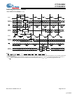
Switching Waveforms (continued)
Q
3
Q
1
Q
0
Q
2
A
0
A
1
A
2
A
3
A
4
A
5
Q
4
A
0
A
1
A
2
A
3
A
4
A
5
t
SA
t
HA
t
SC
t
HC
t
SA
t
HA
t
SC
t
HC
t
SC
t
HC
t
SC
t
HC
t
CKHZ
t
DC
t
DC
t
CD2
t
CKLZ
t
CD2
t
CD2
t
CKHZ
t
CKLZ
t
CD2
t
CKHZ
t
CKLZ
t
CD2
t
CH2
t
CL2
t
CYC2
CLK
ADDRESS
(B1)
CE
(B1)
DATA
OUT(B2)
DATA
OUT(B1)
ADDRESS
(B2)
CE
(B2)
t
CYC2
t
CL2
t
CH2
t
HC
t
SC
t
HW
t
SW
t
HA
t
SA
t
HW
t
SW
t
CD2
t
CKHZ
t
SD
t
HD
t
CKLZ
t
CD2
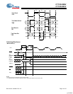
No Operation WriteRead Read
CLK
CE
R/W
ADDRESS
DATA
IN
DATA
OUT
A
n
A
n+1
A
n+2
A
n+2
D
n+2
A
n+3
A
n+4
Q
n
Q
n+3
[+] Feedback