


CY7C0430BV
CY7C0430CV
Document #: 38-06027 Rev. *B Page 27 of 37
The EXTEST, and SAMPLE/PRELOAD instructions can be
used to capture the contents of the Input and Output ring.
Identification (ID) Register
The ID register is loaded with a vendor-specific, 32-bit code
during the Capture-DR state when the IDCODE command is
loaded in the instruction register. The IDCODE is hardwired
into the QuadPort DSE device and can be shifted out when the
TAP controller is in the Shift-DR state. The ID register has a
vendor code and other information described in the Identifi-
cation Register Definitions table.
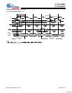
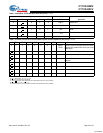
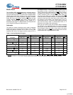
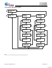
TAP Instruction Set
Sixteen different instructions are possible with the 4-bit
instruction register. All combinations are listed in Table 6,
Instruction Codes. Seven of these instructions (codes) are
listed as RESERVED and should not be used. The other nine
instructions are described in detail below.
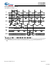
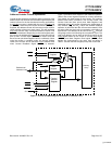
The TAP controller used in this QuadPort DSE device is fully
compatible
[52]
with the 1149.1 convention. The TAP controller
can be used to load address, data or control signals into the
QuadPort DSE device and can preload the Input or output
buffers. The QuadPort DSE device implements all of the
1149.1 instructions except INTEST. Table 6 lists all instruc-
tions.
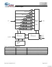
Instructions are loaded into the TAP controller during the
Shift-IR state when the instruction register is placed between
TDI and TDO. During this state, instructions are shifted
through the instruction register through the TDI and TDO pins.
To execute the instruction once it is shifted in, the TAP
controller needs to be moved into the Update-IR state.
EXTEST
EXTEST is a mandatory 1149.1 instruction which is to be
executed whenever the instruction register is loaded with all 0s.
EXTEST allows circuitry external to the QuadPort DSE device
package to be tested. Boundary-scan register cells at output pins
are used to apply test stimuli, while those at input pins capture
test results.
IDCODE
The IDCODE instruction causes a vendor-specific, 32-bit code
to be loaded into the identification register. It also places the
identification register between the TDI and TDO pins and
allows the IDCODE to be shifted out of the device when the
TAP controller enters the Shift-DR state. The IDCODE
instruction is loaded into the instruction register upon
power-up or whenever the TAP controller is given a test logic
reset state.
High-Z
The High-Z instruction causes the bypass register to be
connected between the TDI and TDO pins when the TAP
controller is in a Shift-DR state. It also places all QuadPort
DSE device outputs into a High-Z state.
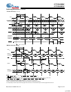
SAMPLE/PRELOAD
SAMPLE/PRELOAD is a 1149.1 mandatory instruction. When
the SAMPLE/PRELOAD instructions loaded into the
instruction register and the TAP controller in the Capture-DR
state, a snapshot of data on the inputs and output pins is
captured in the boundary scan register.
The user must be aware that the TAP controller clock can only
operate at a frequency up to 10 MHz, while the QuadPort DSE
device clock operates more than an order of magnitude faster.
Because there is a large difference in the clock frequencies, it
is possible that during the Capture-DR state, an input or output
will undergo a transition. The TAP may then try to capture a
signal while in transition (metastable state). This will not harm
the device, but there is no guarantee as to the value that will
be captured. Repeatable results may not be possible.
To guarantee that the boundary scan register will capture the
correct value of a signal, the QuadPort DSE device signal
must be stabilized long enough to meet the TAP controller’s
capture set-up plus hold times. Once the data is captured, it is
possible to shift out the data by putting the TAP into the
Shift-DR state. This places the boundary scan register
between the TDI and TDO pins. If the TAP controller goes into
the Update-DR state, the sampled data will be updated.
BYPASS
When the BYPASS instruction is loaded in the instruction
register and the TAP is placed in a Shift-DR state, the bypass
register is placed between the TDI and TDO pins. The
advantage of the BYPASS instruction is that it shortens the
boundary scan path when multiple devices are connected
together on a board.
CLAMP
The optional CLAMP instruction allows the state of the signals
driven from QuadPort DSE device pins to be determined from
the boundary-scan register while the BYPASS register is
selected as the serial path between TDI and TDO. CLAMP
controls boundary cells to 1 or 0.
CYBIST
CYBIST instruction provides the user with a means of running
a user-accessible self-test function within the QuadPort DSE
device as a result of a single instruction. This permits all
components on a board that offer the CYBIST instruction to
execute their self-tests concurrently, providing a quick check
for the board. The QuadPort DSE device MBIST provides two
modes of operation once the TAP controller is loaded with the
CYBIST instruction:
Non-Debug Mode (Go-NoGo)
The non-debug mode is a go-nogo test used simply to run
BIST and obtain pass-fail information after the test is run. In
addition to that, the total number of failures encountered can
be obtained. This information is used to aid the debug mode
(explained next) of operation. The pass-fail information and
failure count is scanned out using the JTAG interface. An
MBIST Result Register (MRR) will be used to store the
pass-fail results. The MRR is a 25-bit register that will be
connected between TDI and TDO during the internal scan
(INT_SCAN) operation. The MRR will contain the total number
of fail read cycles of the entire MBIST sequence. MRR[0] (bit
0) is the Pass/Fail bit. A “1” indicates some type of failure
occurred, and a “0” indicates entire memory pass.
In order to run BIST in non-debug mode, the two-bit MBIST
Control Register (MCR) is loaded with the default value “00”,
and the TAP controller’s finite state machine (FSM), which is
synchronous to TCK, transitions to Run Test/Idle state. The
entire MBIST test will be performed with a deterministic
[+] Feedback