CY7C63413C
CY7C63513C
CY7C63613C
Document #: 38-08027 Rev. *B Page 11 of 32
initialization noted under “Reset,” bit 6 of the Processor Status
and Control Register is set to “1” to indicate to the firmware
that a Watch Dog Reset occurred.
The Watch Dog Timer is a 2-bit timer clocked by a 4.096-ms
clock (bit 11) from the free-running timer. Writing any value to
the write-only Watch Dog Clear I/O port (0x26) will clear the
Watch Dog Timer.
In some applications, the Watch Dog Timer may be cleared in
the 1.024-ms timer interrupt service routine. If the 1.024-ms
timer interrupt service routine does not get executed for 8.192
ms or more, a Watch Dog Timer Reset will occur. A Watch Dog
Timer Reset lasts for 2.048 ms after which the microcontroller
begins execution at ROM address 0x0000. The USB trans-
mitter is disabled by a Watch Dog Reset because the USB
Device Address Register is cleared. Otherwise, the USB
Controller would respond to all address 0 transactions. The
USB transmitter remains disabled until the MSB of the USB
address register is set.
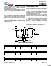
General Purpose I/O Ports
Ports 0 to 2 provide 24 GPIO pins that can be read or written.
Each port (8 bits) can be configured as inputs with internal pull-
ups, open drain outputs, or traditional CMOS outputs. Please
note an open drain output is also a high-impedance (no pull-
up) input. All of the I/O pins within a given port have the same
configuration. Ports 0 to 2 are considered low current drive
with typical current sink capability of 7 mA.
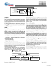
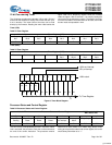
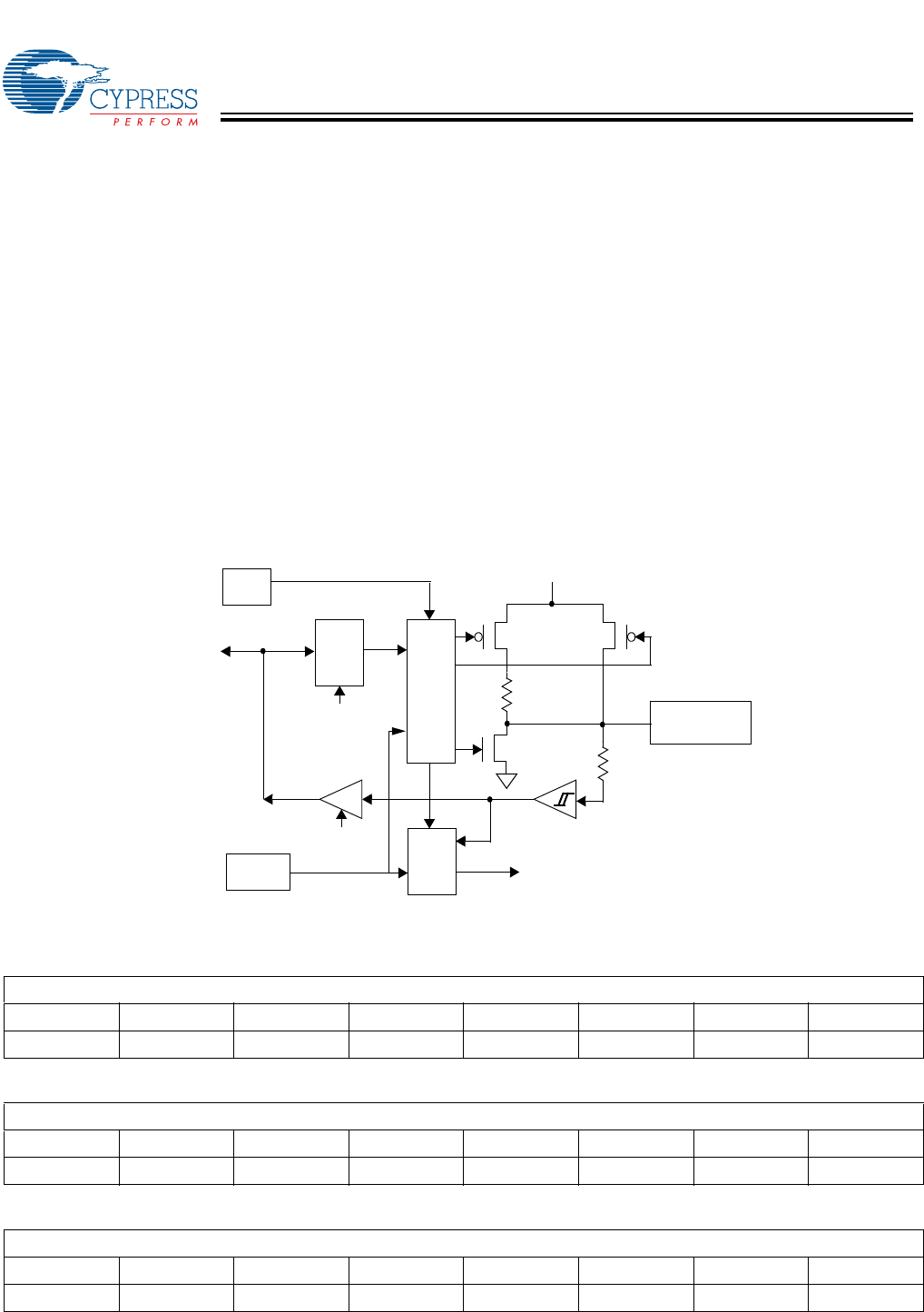
The internal pull-up resistors are typically 7 kΩ. Two factors
govern the enabling and disabling of the internal pull-up
resistors: the port configuration selected in the GPIO Configu-
ration register and the state of the output data bit. If the GPIO
Configuration selected is “Resistive” and the output data bit is
“1,” then the internal pull-up resistor is enabled for that GPIO
pin. Otherwise, Q1 is turned off and the 7-kΩ pull-up is
disabled. Q2 is “ON” to sink current whenever the output data
bit is written as a “0.” Q3 provides “HIGH” source current when
the GPIO port is configured for CMOS outputs and the output
data bit is written as a “1”. Q2 and Q3 are sized to sink and
source, respectively, roughly the same amount of current to
support traditional CMOS outputs with symmetric drive.
.
Figure 4. Block Diagram of a GPIO Line
GPIO
Pin
V
CC
7 kΩ
ESD
GPIO
CFG
mode
2 bits
Data
Out
Latch
Internal
Data Bus
Port Read
Port Write
Interrupt
Enable
Control
Control
to Interrupt
Controller
Q1
Q2
Q3
Internal
Buffer
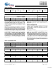
Table 2. Port 0 Data
Addr: 0x00 Port 0 Data
P0[7] P0[6] P0[5] P0[4] P0[3] P0[2] P0[1] P0[0]
R/W R/W R/W R/W R/W R/W R/W R/W
Table 3. Port 1 Data
Addr: 0x01 Port 1 Data
P1[7] P1[6] P1[5] P1[4] P1[3] P1[2] P1[1] P1[0]
R/W R/W R/W R/W R/W R/W R/W R/W
Table 4. Port 2 Data
Addr: 0x02 Port 2 Data
P2[7] P2[6] P2[5] P2[4] P2[3] P2[2] P2[1] P2[0]
R/W R/W R/W R/W R/W R/W R/W R/W
[+] Feedback


