CY7C68000A
Document #: 38-08052 Rev. *G Page 2 of 15
Applications
Mobile Applications
■ Smart Phones
■ PDA Phones
■ Gaming Phones
■ MP3 players
■ Portable Media Players (PMP)
■ GPS Tracking Devices
Consumer Applications
■ Cameras
■ Scanners
■ DSL Modems
■ Memory Card Readers
Non-Consumer Applications
■ Networking
■ Wireless LAN
■ Home PNA
Functional Overview
The functionality of this chip is described in the following
sections:
USB Signaling Speed
The MoBL-USB TX2 operates at two of the rates defined in the
USB Specification 2.0, dated 4/27/2000.
■ Full speed, with a signaling bit rate of 12 Mbps
■ High speed, with a signaling bit rate of 480 Mbps
The MoBL-USB TX2 does not support the LS signaling rate of
1.5 Mbps.
Transceiver Clock Frequency
The MoBL-USB TX2 has an on-chip oscillator circuit that uses
an external 24 MHz (±100 ppm) crystal with the following charac-
teristics:
■ Parallel resonant
■ Fundamental mode
■ 500 μW drive level
■ 27 to 33 pF (5% tolerance) load capacitors
An on-chip phase-locked loop (PLL) multiplies the 24 MHz oscil-
lator up to 30 or 60 MHz, as required by the transceiver parallel
data bus. The default UTMI interface clock (CLK) frequency is
determined by the DataBus16_8 pin.
Buses
The two packages enable a 8- or 16-bit bidirectional data bus for
data transfers to a controlling unit.
Suspend and Tri-state Modes
When the MoBL-USB TX2 is not in use, the processor reduces
power consumption by putting it into Suspend mode using the
Suspend pin.
While in Suspend mode, Tri-state mode may be enabled, which
tri-states all outputs and IOs, enabling the UTMI interface pins to
be shared with other devices. This is valuable in mobile handset
applications, where GPIOs are at a premium. The outputs and
IOs are tri-stated ~50ns when Tri-state mode is enabled, and are
driven ~50ns when Tri-state mode is disabled. All inputs must not
be left floating while in Tri-state mode.
When resuming after a suspend, the PLL stabilizes approxi-
mately 200 μs after the suspend pin goes high.
Reset Pin
An input pin (Reset) resets the chip. This pin has hysteresis and
is active HIGH according to the UTMI specification. The internal
PLL stabilizes approximately 200 μs after V
CC
has reached 3.3V.
Line State
The Line State output pins LineState[1:0] are driven by combina-
tional logic and may be toggling between the ‘J’ and the ‘K’
states. They are synchronized to the CLK signal for a valid
signal. On the CLK edge, the state of these lines reflect the state
of the USB data lines. Upon the clock edge the ‘0’ bit of the
LineState pins is the state of the DPLUS line and the ‘1’ bit of
LineState is the DMINUS line. When synchronized, the setup
and hold timing of the LineState is identical to the parallel data
bus.
Full-speed versus High-speed Select
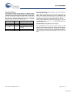
The FS versus HS is done through the use of both XcvrSelect
and the TermSelect input signals. The TermSelect signal enables
the 1.5 Kohm pull up on to the DPLUS pin. When TermSelect is
driven LOW, a SE0 is asserted on the USB providing the HS
termination and generating the HS Idle state on the bus. The
XcvrSelect signal is the control that selects either the FS trans-
ceivers or the HS transceivers. By setting this pin to a ‘0’ the HS
transceivers are selected and by setting this bit to a’1’ the FS
transceivers are selected.
[+] Feedback


