CY8C24123A
CY8C24223A, CY8C24423A
Document Number: 38-12028 Rev. *I Page 11 of 56
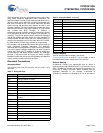
32-Pin Part Pinout
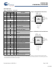
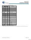
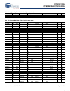
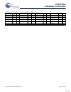
Table 6. Pin Definitions - 32-Pin QFN**
Pin
No.
Type
Pin
Name
Description
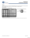
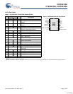
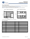
Figure 8. CY8C24423A 32-Pin PSoC Device
Digital Analog
1 IO P2[7]
2 IO P2[5]
3 IO I P2[3] Direct Switched Capacitor Block Input
4 IO I P2[1] Direct Switched Capacitor Block Input
5 Power Vss Ground Connection
6 Power SMP Switch Mode Pump (SMP) Connection
to External Components required
7 IO P1[7] I2C Serial Clock (SCL).
8 IO P1[5] I2C Serial Data (SDA).
9 NC No Connection
10 IO P1[3]
11 IO P1[1] Crystal Input (XTALin), I2C Serial Clock
(SCL), ISSP-SCLK*
12 Power Vss Ground Connection
13 IO P1[0] Crystal Output (XTALout), I2C Serial
Data (SDA), ISSP-SDATA*
14 IO P1[2]
15 IO P1[4] Optional External Clock Input
(EXTCLK)
16 NC No Connection
17 IO P1[6]
18 Input XRES Active High External Reset with Internal
Pull Down
19 IO I P2[0] Direct Switched Capacitor Block Input
20 IO I P2[2] Direct Switched Capacitor Block Input
21 IO P2[4] External Analog Ground (AGND)
22 IO P2[6] External Voltage Reference (VRef)
23 IO I P0[0] Analog Column Mux Input
24 IO I P0[2] Analog Column Mux Input
25 NC No Connection
26 IO I P0[4] Analog Column Mux Input
27 IO I P0[6] Analog Column Mux Input
28 Power Vdd Supply Voltage
29 IO I P0[7] Analog Column Mux Input
30 IO IO P0[5] Analog Column Mux Input and Column
Output
31 IO IO P0[3] Analog Column Mux Input and Column
Output
32 IO I P0[1] Analog Column Mux Input
LEGEND: A = Analog, I = Input, and O = Output.
* These are the ISSP pins, which are not High Z at POR (Power On Reset). See the PSoC Programmable Sytem-on-Chip Technical Reference Manual for details.
** The center pad on the QFN package must be connected to ground (Vss) for best mechanical, thermal, and electrical performance. If not connected to ground, it must
be electrically floated and not connected to any other signal.
P2[7]
P2[5]
A, I, P2[3]
A, I, P2[1]
Vss
SMP
QFN
(Top View)
9
10
11
12
13
14
15
16
1
2
3
4
5
6
7
8
24
23
22
21
20
19
18
17
32
31
30
29
28
27
26
25
P0[1], A, I
P0[3], A, IO
P0[5], A, IO
P0[7], A, I
Vdd
P0[6], A, I
P0[4], A, I
NC
I2C SCL, P1[7]
I2C SDA, P1[5]
P0[2], A, I
P0[0], A, I
XRES
P1[6]
NC
P1[3]
I2C SCL, XTALin, P1[1]
Vss
I2C SDA, XTALout, P1[0]
P1[2]
EXTCLK, P1[4]
NC
P2[6], External VRef
P2[4], External AGND
P2[2], A, I
P2[0], A, I
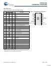
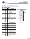
P2[7]
P2[5]
A, I, P2[3]
A, I, P2[1]
Vss
SMP
QFN
(Top View)
9
10
11
12
13
14
15
16
1
2
3
4
5
6
7
8
24
23
22
21
20
19
18
17
32
31
30
29
28
27
26
25
P0[1], A, I
P0[3], A, IO
P0[7], A, I
Vdd
P0[6], A, I
P0[4], A, I
NC
12 CS CL, P1[7]
12 CS DA, P1[5]
P0[2], A, I
P0[0], A, I
XRES
P1[6]
NC
P1[3]
12 CS CL, XTALin, P1[1]
Vss
12 CS DA, XTALout, P1[0]
P1[2]
EXTCLK, P1[4]
NC
P2[6], ExternalVRef
P2[4], ExternalA GND
P2[2], A, I
P2[0], A, I
P0[5], A, IO
Figure 9. CY8C24423A 32-Pin Sawn PSoC Device
[+] Feedback


