


CY8C24223A, CY8C24423A
Document Number: 3-12029 Rev. *E Page 8 of 31
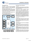
Pinouts
The CY8C24x23A automotive PSoC device is available in a variety of packages which are listed and illustrated in the following tables.
Every port pin (labeled with a “P”) is capable of Digital IO. However, Vss, Vdd, and XRES are not capable of Digital IO.
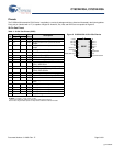
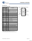
20-Pin Part Pinout
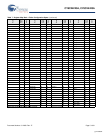
Table 3. 20-Pin Part Pinout (SSOP)
Pin
No.
Type
Pin
Name
Description
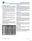
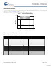
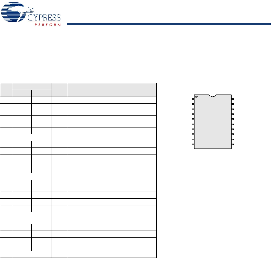
Figure 5. CY8C24223A 20-Pin PSoC Device
Digital Analog
1 IO I P0[7] Analog column mux input
2 IO IO P0[5] Analog column mux input and column
output
3 IO IO P0[3] Analog column mux input and column
output
4 IO I P0[1] Analog column mux input
5 Power Vss Ground connection
6 IO P1[7] I2C Serial Clock (SCL)
7 IO P1[5] I2C Serial Data (SDA)
8 IO P1[3]
9 IO P1[1] Crystal Input (XTALin), I2C Serial Clock
(SCL), ISSP-SCLK*
10 Power Vss Ground connection
11 IO P1[0] Crystal Output (XTALout), I2C Serial Data
(SDA), ISSP-SDATA*
12 IO P1[2]
13 IO P1[4] Optional External Clock Input (EXTCLK)
14 IO P1[6]
15 Input XRES Active high external reset with internal pull
down
16 IO I P0[0] Analog column mux input
17 IO I P0[2] Analog column mux input
18 IO I P0[4] Analog column mux input
19 IO I P0[6] Analog column mux input
20 Power Vdd Supply voltage
LEGEND: A = Analog, I = Input, and O = Output.
* These are the ISSP pins, which are not High Z at POR (Power On Reset).
See the PSoC Programmable System-on-Chip Technical Reference Manual for details.
A, I, P0[7]
A, IO, P0[5]
A, IO, P0[3]
A, I, P0[1]
I2C SCL, P1[7]
I2C SDA, P1 [5 ]
P1[3]
I2C SCL, XTALin, P1[1]
Vss
SSOP
20
19
18
17
16
15
14
13
12
11
1
2
3
4
5
6
7
8
9
10
Vd d
P0[6], A, I
P0[4], A, I
P0[2], A, I
P0[0], A, I
XRES
P1[6]
P1[4], EXTCLK
P1[2]
P1[0], XTALout, I2C SDA
Vss
[+] Feedback