


CYD01S36V
CYD02S36V/36VA/CYD04S36V
CYD09S36V/CYD18S36V
Document Number: 38-06076 Rev. *G Page 16 of 28
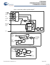
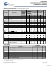
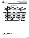
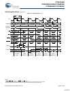
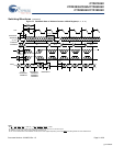
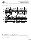
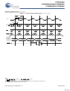
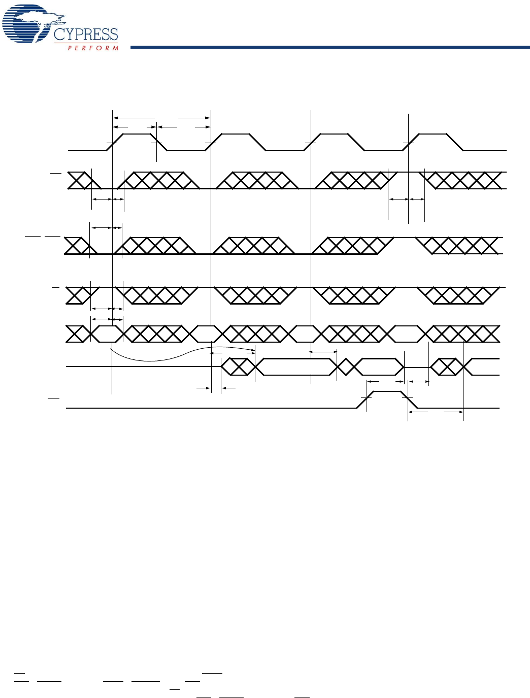
Figure 8. Read Cycle
[14, 33, 34, 35, 36]
Notes
33.OE
is asynchronously controlled; all other inputs (excluding MRST and JTAG) are synchronous to the rising clock edge.
34.ADS
= CNTEN = LOW, and MRST = CNTRST = CNT/MSK = HIGH.
35.The output is disabled (high-impedance state) by CE
= V
IH
following the next rising edge of the clock.
36.Addresses do not have to be accessed sequentially since ADS
= CNTEN = V
IL
with CNT/MSK = V
IH
constantly loads the address on the rising edge of the CLK.
Numbers are for reference only.
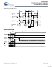
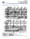
Switching Waveforms (continued)
t
CH2
t
CL2
t
CYC2
t
SC
t
HC
t
SW
t
HW
t
SA
t
HA
A
n
A
n+1
CLK
CE
R/W
ADDRESS
DATA
OUT
OE
A
n+2
A
n+3
t
SC
t
HC
t
OHZ
t
OE
t
OLZ
t
DC
t
CD2
t
CKLZ
Q
n
Q
n+1
Q
n+2
1 Latency
BE0
–BE3
t
SB
t
HB
[+] Feedback