


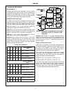

9
INTR (Interrupt Request)
A “high” on this output can be used to interrupt the CPU
when and input device is requesting service. INTR is set by
the condition:
STB is a “one”, IBF is a “one” and INTE is a
“one”. It is reset by the falling edge of
RD. This procedure
allows an input device to request service from the CPU by
simply strobing its data into the port.
INTE A
Controlled by bit set/reset of PC4.
INTE B
Controlled by bit set/reset of PC2.
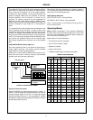
Output Control Signal Definition
(Figure 8 and 9)
OBF - Output Buffer Full F/F). The OBF output will go “low”
to indicate that the CPU has written data out to be specified
port. This does not mean valid data is sent out of the part at
this time since
OBF can go true before data is available.
Data is guaranteed valid at the rising edge of
OBF, (See
Note 1). The
OBF F/F will be set by the rising edge of the
WR input and reset by ACK input being low.
ACK - Acknowledge Input). A “low” on this input informs the
82C55A that the data from Port A or Port B is ready to be
accepted. In essence, a response from the peripheral device
indicating that it is ready to accept data, (See Note 1).
INTR - (Interrupt Request). A “high” on this output can be
used to interrupt the CPU when an output device has
accepted data transmitted by the CPU. INTR is set when
ACK is a “one”, OBF is a “one” and INTE is a “one”. It is
reset by the falling edge of
WR.
INTE A
Controlled by Bit Set/Reset of PC6.
INTE B
Controlled by Bit Set/Reset of PC2.
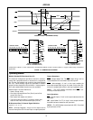
NOTE:
1. To strobe datainto the peripheraldevice, the user mustoperate
the strobe line in a handshaking mode. The user needs to send
OBF to the peripheral device, generates an ACK from the pe-
ripheral device and then latch data into the peripheral device on
the rising edge of OBF.
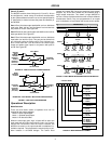
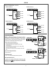
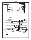
FIGURE 7. MODE 1 (STROBED INPUT)
tST
STB
INTR
RD
INPUT FROM
IBF
PERIPHERAL
tSIB
tSIT
tPH
tPS
tRIT
tRIB
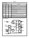
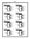
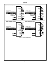
FIGURE 8. MODE 1 OUTPUT
1
D7
0
D6
1
D5
1
D4
1/0
D3
D2 D1 D0
CONTROL WORD
MODE 1 (PORT A)
PC7
8
ACKAPC6
PA7-PA0
OBFA
INTRA
PC3
PC4, PC5
2
WR
PC4, PC5
1 = INPUT
0 = OUTPUT
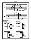
1
D7
D6 D5 D4 D3 D2 D1 D0
CONTROL WORD
MODE 1 (PORT B)
PC1
8
ACKBPC2
INTE
B
PB7-PB0
OBFB
INTRB
PC0
WR
10
INTE
A
82C55A