


RX
-
8581
SA
/
JE
/
NB
Page - 6 MQ372-02
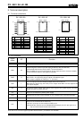
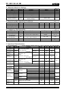
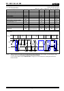
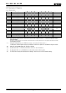
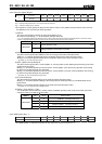
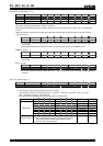
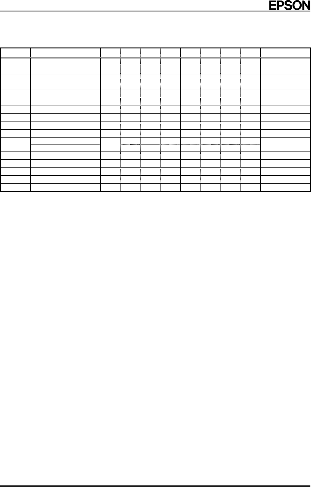
8.2. Description of Registers
8.2.1. Register table
Address Function bit 7 bit 6 bit 5 bit 4 bit 3 bit 2 bit 1 bit 0
Remark
0 SEC
!
40 20 10 8 4 2 1
∗3
1 MIN
!
40 20 10 8 4 2 1
∗3
2 HOUR
!
!
20 10 8 4 2 1
∗3
3 WEEK
!
6 5 4 3 2 1 0
∗3
4 DAY
!
!
20 10 8 4 2 1
∗3
5 MONTH
!
!
!
10 8 4 2 1
∗3
6 YEAR 80 40 20 10 8 4 2 1
−
7 RAM
• • • • • • • •
∗4
8 MIN Alarm AE 40 20 10 8 4 2 1
−
9 HOUR Alarm AE
•
20 10 8 4 2 1
∗4
WEEK Alarm 6 5 4 3 2 1 0
A
DAY Alarm
AE
•
20 10 8 4 2 1
∗4
B Timer Counter 0 128 64 32 16 8 4 2 1
−
C Timer Counter 1
• • • •
2048 1024 512 256
∗4
D Extension Register TEST WADA USEL TE
!
!
TSEL1 TSEL0
∗1, ∗3, ∗5
E Flag Register
!
!
UF TF AF
!
VLF
!
∗1, ∗2, ∗3
F Control Register
!
!
UIE TIE AIE
!
STOP RESET
∗3
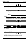
Note
When after the initial power-up or when the result of read out the VLF bit is "1" , initialize all registers, before
using the module.
Be sure to avoid entering incorrect date and time data, as clock operations are not guaranteed when the data
or time data is incorrect.
∗1) During the initial power-up, the TEST bit is reset to "0" and the VLF bit is set to "1".
∗ At this point, all other register values are undefined, so be sure to perform a reset before using the module.
∗2)
Only a "0" can be written to the UF, TF, AF, or VLF bit.
∗3)
Any bit marked with "
!
" should be used with a value of "0" after initialization.
∗4) Any bit marked with "•" is a RAM bit that can be used to read or write any data.
∗5)
The TEST bit is used by the manufacturer for testing. Be sure to set "0" for this bit when writing.