Installing and Configuring the EVGA nForce 680i SLI Motherboard
76
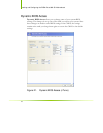
RAS to RAS Delay
The RAS-to-RAS delay (tRRD) is the is the amount of cycles it takes to
activate the next bank of memory (this is the opposite of tRAS). The lower
the timing the better the system performance. However, this scenario can
cause instability. Adjustable from 1 to 15.
Refresh Rate
This value is filled in by the system and can not be changed by the user.
Memory bank switch
The row Precharge time (tRP) is the minimum time between active
commands and the read/writes of the next bank on the memory module.
Adjustable from 1 to 15.
R to W Turnaround
The Read-to-Write turnaround (tRWT) is a the amount of cycles for the
command to be executed when a Write command is received. Adjustable
from 1 to 15.
R to R Timing
the Read-to-Read time (tRDRD) is the number of clock cycles between the
last read and the subsequent READ command to the same physical bank.
Adjustable from 1 to 15.
Row Cycle Time
The Row Cycle Time is the minimum time in cycles it take a row to
complete a full cycle. This can be determined by tRC=tRAS+tRP. If this
value is set too short, it can cause corruption of data. If this value is set too
high, it causes a loss in performance but an increase in stability. Adjustable
from 1 to 63 cycles
W to R Command Delay
The Write-to-Read (tWRD) command delay is the amount of cycles required
between a valid write command and the next read command. A lower cycle
time results in better performance but is can instability. Adjustable from 0 to
6 cycles.
W to W Timing
The Write-to-Write (tWRWR) timing is the number of clock cycles between
the last write and the subsequent Write command to the same physical bank.
Adjustable from 2 to 15 cycles.
CAS Latency
The CAS Latency (tCL) is the time (in number of clock cycles) that elapses
after the memory controller sends a request to read a memory location and
before the data is sent to the module's output pins. The value shown cannot
be changed.


