


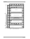
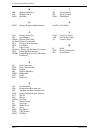
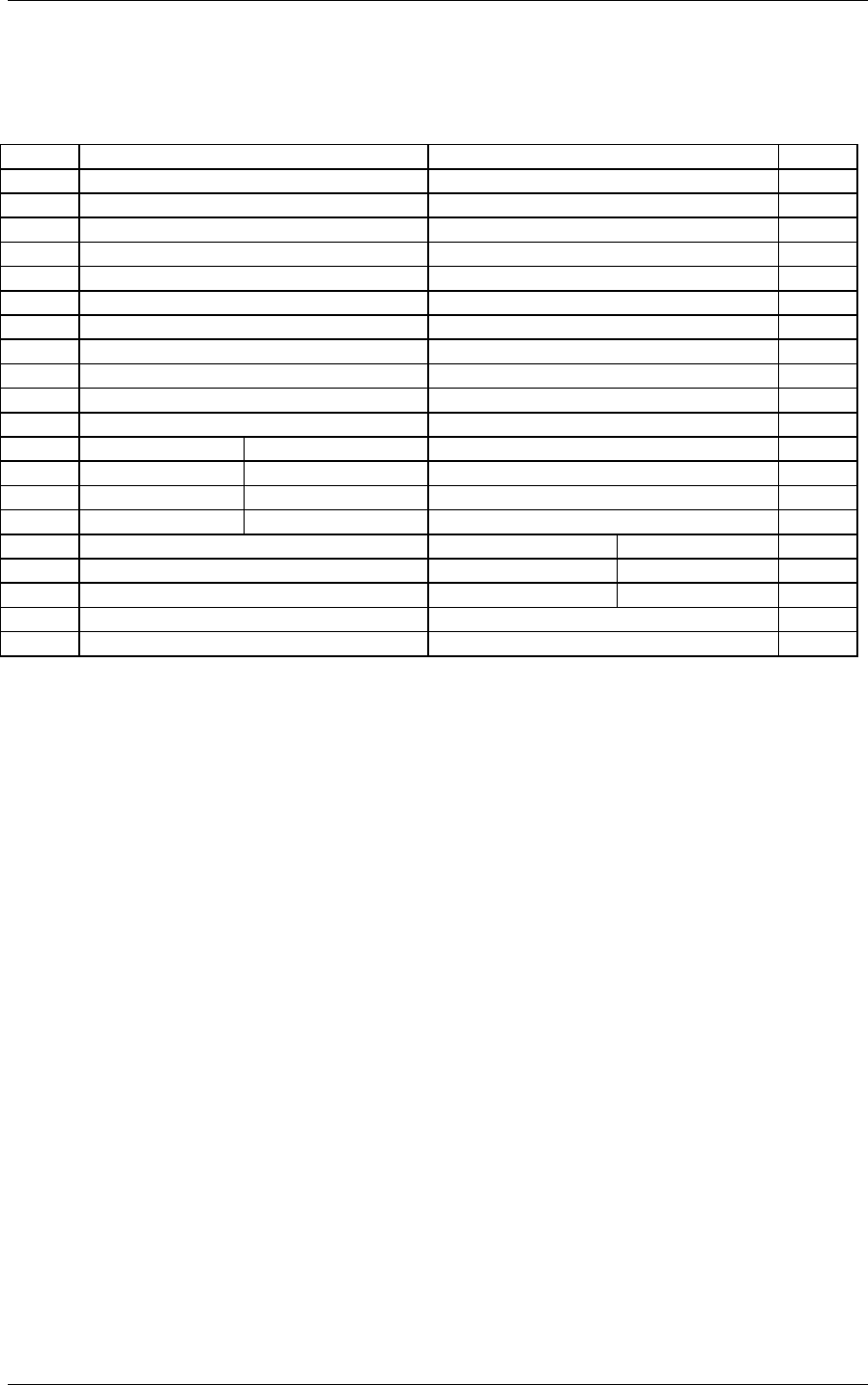
Connector Signal Allocation
A-2 C141-E235
A.1 Interface (FC-SCA) Connector Signal Allocation
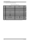
Table A.1 FC-SCA connector: CN1
Pin No. Signal Signal Pin No.
01 –EN bypass port A +12V charge 21
02 +12V GND 22
03 +12V GND 23
04 +12V +PortA_in 24
05 –Parallel ESI –PortA_in 25
06 –Drive present GND 26
07 Active LED out +PortB_in 27
08 –Spindle sync –PortB_in 28
09 Start_1/Mated GND 29
10 Start_2/Mated +PortA_out 30
11 –EN bypass port B –PortA_out 31
12* SEL-6 –DSK_WR GND 32
13* SEL-5 –DSK_RD +PortB-out 33
14* SEL-4 –ENCL_ACK –PortB-out 34
15* SEL-3 D(3) GND 35
16 Fault LED out SEL-2 D(2) 36*
17 DEV_CTRL_CODE2 SEL-1 D(1) 37*
18 DEV_CTRL_CODE1 SEL-0 D(0) 38*
19 +5V DEV_CTRL_CODE0 39
20 +5V +5V charge 40
Note: *1) Signal names in the right column of the table are those in parallel ESI operation.