


13
MB15C02
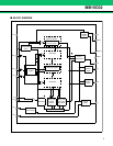
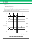
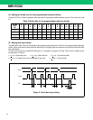
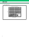
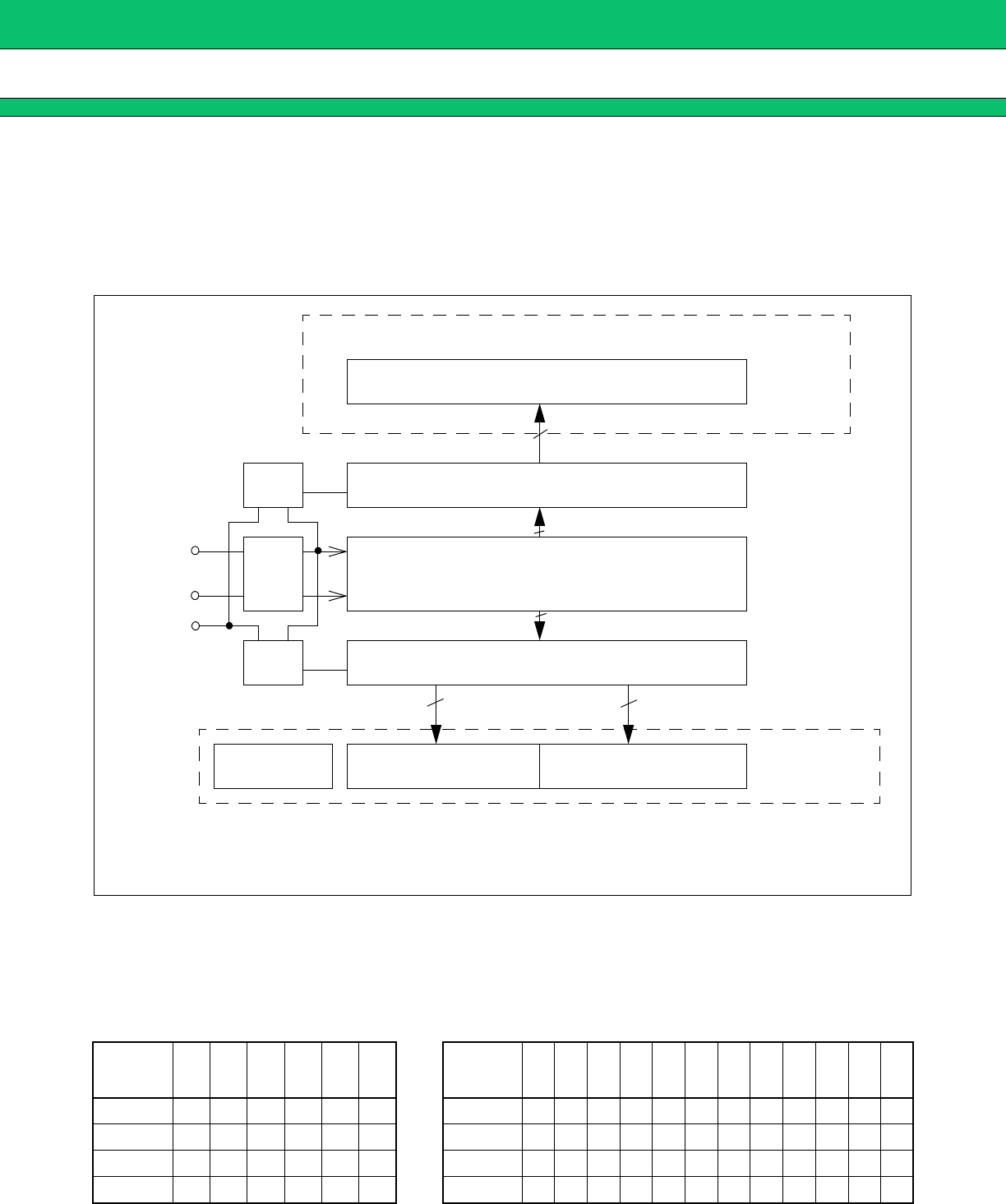
(2) The flow of serial data
Serial data is received via data pin in synchronization with the clock input and loaded into shift register which contains
the divide ratio setting data and into the control register which contains the control bit. The logical product (through
the AND gate in Figure 4) of LE and the control register output (i.e., control bit) is fed to the enable input of the
latches. Accordingly, when LE is set high, the latch for the divider identified by the control bit is enabled and the
divide ratio data from the shift register is loaded into the selected counter (s).
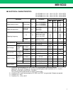
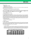
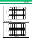
(3) Setting the divide ratio for the programmable divider
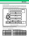
Columns A0 to A5 of Table 2.1 represent the divide ratio of the swallow counter and columns N0 to N11 of Table2.2
represent the divide ratio of programmable counter.
Table. 2 Divide ratio for the programmable divider
Table.2.1 Swallow counter divider A Table2.2 Programmable counter divider N
Note: Less than 5 is prohibited.
Divide
ratio
(A)
A
0
A
1
A
2
A
3
A
4
A
5
Divide
ratio
(N)
N
0
N
1
N
2
N
3
N
4
N
5
N
6
N
7
N
8
N
9
N
10
N
11
0 0 0 0 0 0 0 5 101000000000
1 1 0 0 0 0 0 6 011000000000
⋅ ⋅⋅⋅⋅⋅⋅ ⋅ ⋅⋅⋅⋅⋅⋅⋅⋅⋅⋅⋅⋅
63 1 1 1 1 1 1 4095 111111111111
Figure 4. The flow of serial data
14-bit binary programmable reference counter
Programmable
reference divider
14-bit latch
18-bit shift register
18-bit latch
AND
C*
AND
Data
Clock
LE
Prescaler
6-bit binary swallow counter
12-bit binary programmable
counter
Programmable
divider
* : Control register
612
18
14
14