9
MB15C02
Divide ratio range:
Prescaler : M = 64, M+1=65
Swallow counter : A = 0 to 63
Programmable counter : N = 5 to 4095
The MB15C02 uses the pulse swallow method; consequently, the divide rations of the swallow and programmable
counters must satisfy the relationship N>A.
The total divide ratio of the programmable divider is calculated as follows:
Total divide ratio = (M + 1) × A + M × (N – A) = M × N + A = 64 × N + A
When N is set within 5<
N<63, the possible divide ratio A of the swallow counter can take values 0<A<N-1 because
N must be greater than A. For example, 0<
A<19 is allowed when N=20 but 20<A<63 is not allowed in that case.
Consequently, N>
64 must be satisfied for the total divider to be set within 0<A<63.
The fp and fin have the following relation:
fp = fin / (64 × N + A)
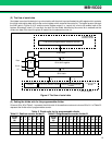
(3) Programmable reference divider
The programmable reference divider divides the reference oscillation frequency(fosc) from the crystal oscillator
connected between OSCin and OSCout pins or from the external oscillator input taken in directly through OSCin,
pin and then, sends the resultant fr to the phase comparator. It consists of a 14-bit binary programmable reference
counter. When the output from the external oscillator is to be input directly to OSCin, pin the connection must be
AC coupled and OSCout pin is left open. Also, to prevent OSCout from malfunctioning, its traces on the printed
circuit board must be kept minimal or eliminated entirely; whenever possible, it must be free of any form of load.
The following divider is used:
Programmable reference counter : R = 5 to 16383
The fr and f
osc have the following relation:
fr = fosc / R
(4) Phase comparator
The phase comparator detects the phase difference between the outputs fr and fp from the dividers and generates
an error signal that is proportional to phase difference. The outputs from the phase comparator include 1) Do which
takes on one of the three states, namely, “L” (low), “H” (high), and “Z” (high impedance), and is sent to the LPF,
2)φR, 3)φP, 4)LD which indicates the PLL lock or unlock states.
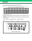
(a) Phase comparator
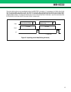
The phase comparator detects the phase error between fr and fp, then generates an error signal that is
proportional to the phase error. The roles of the fr and fp supplied to the phase comparator may be reversed
by switching the logical input level of pin FC. This inverts the logical level of the Do output. The logical level of
Do output may be selected according to the characteristics of the external LPF and the VCO. (Refer to Table 1.)
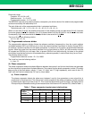
Table. 1 Phase comparator inputs/output relationships
FC = “L” FC = “H”
Do φR φPDoφR φP
fr > fp H L L L H Z
fr = fp Z L Z Z L Z
fr < fp L H Z H L L
Output
Phase
relation


