3
MB15C02
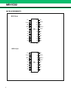
■ PIN DESCRIPTIONS
(Continued)
Pin no.
Pin
name
I/O Descriptions
SSOP
16
SSOP
20
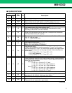
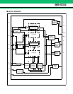
1 1 VDD – Power supply voltage
2 2 Clock I
Clock input for the shift register.(Schmitt trigger input)
Data is shifted into the shift register on the rising edge of the clock.
– 3 NC – No connection
3 4 Data I Serial data input using binary code.(Schmitt trigger input)
4 5 LE I
Load enable signal input (Schmitt trigger input)
When LE is high, the data in the shift register is transferred to a latch,
according to the control bit in the serial data.
5 6 fin I
Prescaler input.
A bias circuit and amplifier are at input port. Connection with an external
VCO should be done by AC coupling.
6 7 PS I
Power saving mode control. This pin must be set at “L” at Power-ON.
PS = “H” ; Normal mode
PS = “L” ; Power saving mode
– 8 NC – No connection
7 9 LD O
Lock detector signal output.
When a PLL is locking, LD outputs “H”.
When a PLL is not locking, LD outputs “L”.
8 10 Do O
Charge pump output.
Phase of the charge pump can be reversed by FC input. The Do output
may be inverted by FC input. The relationships between the programmable
reference divider output (fr) and the programmable divider output (fp) are
shown below;
fr > fp :“H” level (FC = “L”), “L” level (FC = “H”)
fr = fp : High impedance
fr < fp :“L” level (FC = “L”), “H” level (FC = “H”)
9 11 Vp – Power supply for the charge pump.
10 12 φR O
Phase comparator output pin (for external charge pump). Relation between
the programmable reference divider output (fr) and the programmable divider
output (fp) are shown below;
When FC = “L”
fr > fp : φR = “L” level, φP = “L” level
fr = fp : φR = “L” level, φP = High impedance
fr < fp : φR = “H” level, φP = High impedance
When FC = “H”
fr > fp : φR = “H” level, φP = High impedance
fr = fp : φR = “L” level, φP = High impedance
fr < fp : φR = “L” level, φP = “L” level
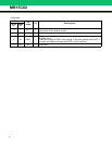
– 13 NC – No connection
11 14 φP O
Phase comparator output pin (for external charge pump). Refer to Pin
description for φR. φP pin is a Nch open drain output.
12 15 FC I Phase comparator input select pin.
13 16 TEST I
Test mode select pin. (Pull down resistor)
Please set this pin to ground or open usually.


