


7
MB15C02
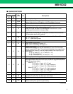
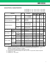
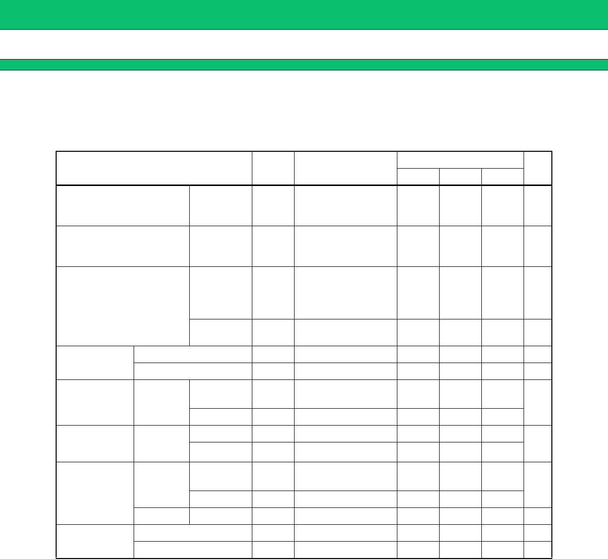
■ ELECTRICAL CHARACTERISTICS
(For 220 MHz :VDD = Vp = 1.0 to 1.5 V, Ta = –20 to +60°C)
(For 330 MHz :V
DD = Vp = 1.2 to 1.5 V, Ta = –20 to +60°C)
(For 450 MHz :V
DD = Vp = 1.3 to 1.5 V, Ta = –20 to +60°C)
*1: Conditions; Inputs except for fin, OSC
IN and TEST are grounded, Outputs are opened.
Specifying the current flowing in V
DD and Vp at operating state under conditions of VDD = Vp, fin =
220 MHz, or 330 MHz, and OSCIN = 12.8 MHz.
The current at locking state shows I
DD Supply current (P.20).
*2: Conditions; PS = Low, Inputs except for fin, OSC
IN and TEST are grounded, Outputs are opened.
*3: Condition; Ta = 25°C
*4: Condition; Ta = –20 to +60°C
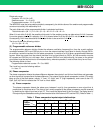
Parameter Symbol Condition
Value
Unit
Min.
Typ.
*3
Max.
*4
Power supply current Active Mode
I
DD
*1
(VDD=1.0V/220MHz)
(V
DD=1.2V/330MHz)
(V
DD=1.3V/450MHz)
–
–
–
0.6
1.0
1.3
1.2
1.8
2.2
mA
Power saving current
Power sav-
ing mode
I
DDS
*2
(VDD=1.0V)
(VDD=1.2V)
(V
DD=1.3V)
–
–
–
50
70
80
250
300
350
µA
Operating frequency
fin fin
Programmable divider
(V
DD=1.0 to 1.5V)
(V
DD=1.2 to 1.5V)
(V
DD=1.3 to 1.5V)
10
10
10
–
–
–
220
330
450
MHz
OSC
IN fOSC
Programmable
reference divider
5–20MHz
Input sensitivity
fin Vfin AC coupling –2.0 – – dBm
OSCin V
OSC AC coupling –2.0 – – dBm
Input voltage
Except for
fin and
OSCin
H level V
IH –
V
DD –
0.2
––
V
L level V
IL ––– 0.2
Input current
Except for
fin, OSCin
and TEST
H level I
IH VIN=VDD ––+1.0
µA
L level I
IL VIN=GND –1.0 – –
Output voltage
Except for
OSC
OUT
and φP
H level V
OH IOH = –0.2 mA
V
DD –
0.2
––
V
L level V
OL IOL = 0.2 mA – – 0.2
φPL levelV
OL IOL = 0.2 mA – – 0.2 V
High impedance
cutoff current
Do I
OFF1 VOUT = GND to VP –100 – 100 nA
φPI
OFF2 VOUT = VDD ––100nA