Interface
5-4 C141-E042-01EN
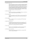
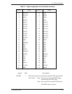
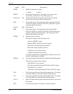
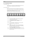
[signal] [I/O] [Description]
MSTR I MSTR, I, Master/slave setting
1: Master 0: Slave
RESET- I Reset signal from the host. This signal is low active and is
asserted for a minimum of 25 ms during power on.
DATA 0-15 I/O Sixteen-bit bi-directional data bus between the host and the
device. These signals are used for data transfer
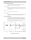
IOW- I Write strobe signal. The rising edge of this signal gates DATA0
to DATA15 signals or DATA0 to DATA7 signals into a register
or the data port on the device.
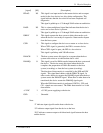
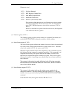
[signal] [I/O] [Description]
IOR- I Read strobe signal. The falling edge of this signal enables
DATA0 to DATA15 or DATA0 to DATA7 data from the device
register or data port onto the data bus. The rising edge of this
signal latches the data at the host.
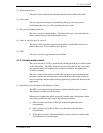
INTRQ O Interrupt signal to the host.
This signal is negated in the following cases:
−
assertion of RESET- signal
−
Reset by SRST of the Device Control register
−
Write to the command register by the host
−
Read of the status register by the host
−
Completion of sector data transfer
(without reading the Status register)
The signal output line has a high impedance when no devices are
selected or interruption is disabled.
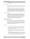
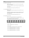
IOCS16- O This signal indicates 16-bit data bus is addressed in PIO data transfer.
This signal is an open collector output.
−
When IOCS16- is not asserted:
8 bit data is transferred through DATA0 to DATA7 signals.
−
When IOCS16- is asserted:
16 bit data is transferred through DATA0 to DATA15 signals.
CS0- I Chip select signal decoded from the host address bus. This signal
is used by the host to select the command block registers.
CS1- I Chip select signal decoded from the host address bus. This signal
is used by the host to select the control block registers.
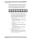
DA 0-2 I Binary decoded address signals asserted by the host to access task
file registers.
KEY - Key pin for prevention of erroneous connector insertion


