


RCV56HCF PCI/CardBus Modem Designer’s Guide
1129
ROCKWELL PROPRIETARY INFORMATION
5-3
5.1.5 Revision ID Field
Initial part hardwired to 00.
5.1.6 Class Code Field
Hardwired to 0x078000 to indicate communications controller.
5.1.7 Latency Timer Register
The Latency Timer register specifies, in units of PCI bus clocks, the value of the Latency Timer for this PCI bus master. This
register has 5 read/write bits (MSBs) plus 3 bits of hardwired zero (LSBs). The Latency Timer Register is loaded into the PCI
Latency counter each time FRAME# is asserted to determine how long the master is allowed to retain control of the PCI bus.
This register is loaded by system software. The default value for Latency Timer is 00.
5.1.8 Header Type Field
Hardwired to 00.
5.1.9 CIS Pointer Register
This register points to the CIS memory located in the BIF’s memory space.
5.1.10 Subsystem Vendor ID and Subsystem ID Registers
Subsystem Vendor ID and Subsystem ID are optional registers that are implemented in this design. Both registers are
loaded from the serial EEPROM after RST#.
5.1.11 Interrupt Line Register
The Interrupt Line register is an eight bit register that is read/write. POST software will write the value of this register as it
initializes and configures the system. The value in this register indicates which of the system interrupt controllers the device’s
interrupt pin is connected to.
5.1.12 Interrupt Pin Register
The Interrupt Pin register tells which interrupt pin the device uses. The value of this register will be 0x01, indicating that
INTA# will be used.
5.1.13 Min Grant and Max Latency Registers
The Min Grant and Max Latency registers are used to specify the devices desired settings for Latency Timer values. For
both registers, the value specifies a period of time in units of ¼ microsecond. Min Grant is used for specifying the desired
burst period assuming a 33 MHz clock. Min Latency specifies how often the device needs to gain access to the PCI bus.
These registers are loaded from the serial EEPROM after RST#.
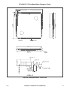
5.2 BASE ADDRESS REGISTER
BIF provides a single Base Address Register. The Base Address Register is a 32 bit register that is used to access the BIF
register set. Bits 3:0 are hard-wired to 0 to indicate memory space. Bits 15-4 will be hard-wired to 0. The remaining bits (31 -
16) will be read/write. This specifies that this device requires a 64k byte address space. After reset, the Base Address
Register contains 0x00000000.
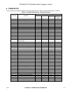
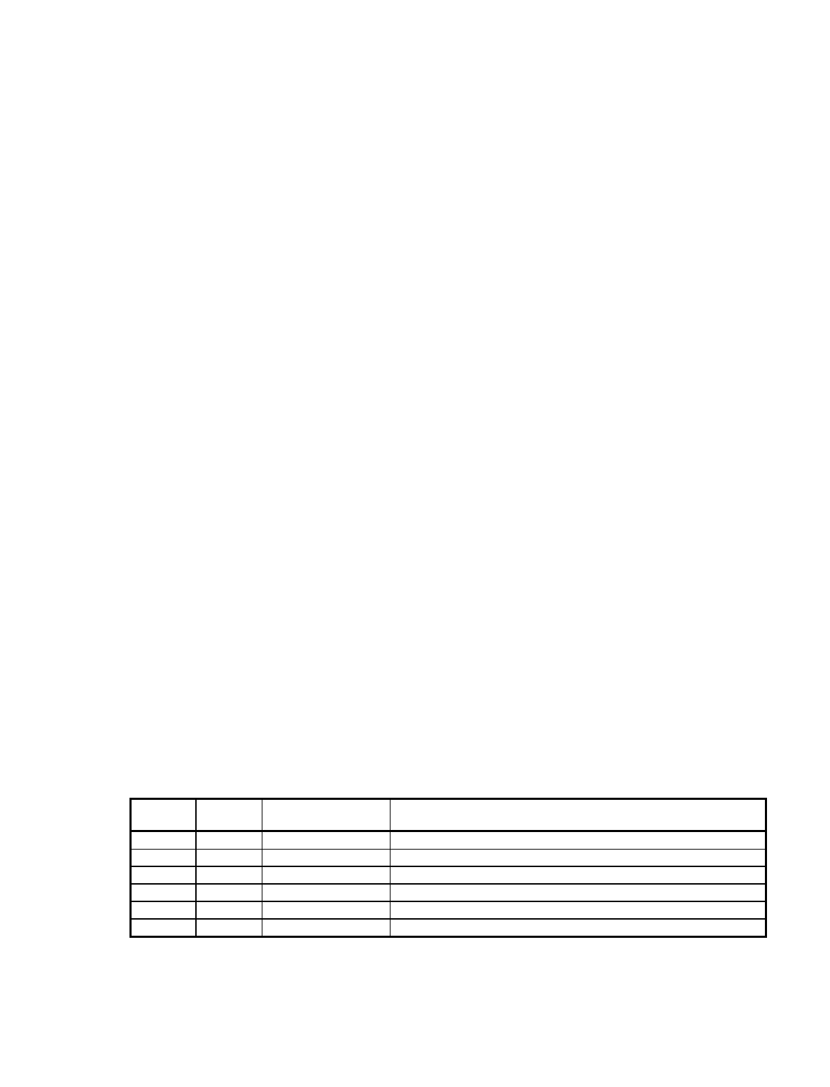
The 64k byte address space used by the BIF is divided into 4k byte regions. Each 4k byte region is used as Table 5-4.
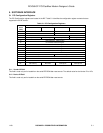
Table 5-4. BIF Address Map
Address
[15:12]
Address
[11:0]
Region Name Description
0x0 0x0-0xfff BASIC2 Registers Buffers, control, and status registers
0x1 0x0-0xfff CIS Memory Data loaded from Serial EEPROM for Card Bus applications
0x2 0x0-0xfff DSP Scratch Pad Access to DSP scratch page registers
0x3 0x0-0xfff Reserved
0x4 0x0-0xfff Reserved
0x5-0xf 0x0-0xfff Reserved.