


Commands184
04h This mode is used to transfer new firmware to the drive. The drive receives
Allocation Length bytes of data from the host. The data is stored in the drive’s
buffer.The location in the buffer at which the data is written is determined by
the firmware.
The firmware image is divided into a number of blocks of data which are sent
to the drive using multiple Write Buffer commands.
All the firmware image data should be transferred using this mode.
The Buffer ID and Buffer Offset are ignored.
05h This mode is used to indicate that the complete firmware image has been sent
to the drive. This is the signal for entering the FLASH reprogramming stage of
the firmware upgrade process.
Once this command has been received, and the associated data stored in the
buffer, the resident firmware checks the validity of the image that has been
received. If this seems to be correct, the Firmware Upgrade operation will
commence. If any faults are detected in the format of the image, the drive will
report CHECK CONDITION to the host. The sense key is ABORTED
COMMAND, and the additional sense is set to 2600h (invalid field in
parameter list).
CAUTION: Once this command has been sent and completed, the
drive’s power supply must not be interrupted until the drive has
completed the firmware upgrade.
The Buffer ID and Buffer Offset are ignored.
0Ah/
1Ah
This mode is used to write to the Echo Buffer.
The Buffer ID and Offset are ignored.
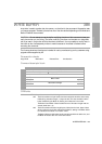
Buffer ID Specifies which buffer to read.
00h
01h
02h
13h
20h
21h
22h
23h
24h
25h
26h
27h
Main buffer (RAM) Offset Boundary: 1 byte
Processor addressable memory (RAM) Offset Boundary: 1 byte
SCSI burst buffer (RAM) Offset Boundary: 4 bytes
or FC burst buffer (RAM) Offset boundary: 512 bytes
PCA EEPROM Offset Boundary: 1 byte
Main buffer segment 0 (RAM) — see below for description)
Main buffer segment 1 (RAM) — see below for description)
Main buffer segment 2 (RAM) — see below for description)
Main buffer segment 3 (RAM) — see below for description)
Main buffer segment 4 (RAM) — see below for description)
Main buffer segment 5 (RAM) — see below for description)
Main buffer segment 6 (RAM) — see below for description)
Main buffer segment 7 (RAM) — see below for description)
Buffer Offset Where in the buffer the data should be written. This must be smaller than the size of the
buffer and must obey the specified offset boundary. When downloading new firmware,
this field is ignored.
Parameter List
Length
The amount of data. This must be smaller than the difference between the Buffer Offset
field and the size of the buffer.