


HONEYWELL Aerospace Electronic Systems Page 47
Use or disclosure of information on this page is subject to the restrictions on the title page of this document.
5 HARDWARE DESCRIPTION
5.1 Mechanical Design
The MARK III is a modular design that consists of a number of circuit card assemblies (CCAs) which are
enclosed in a lightweight aluminum chassis. The internal interconnect between circuit card assemblies
consists of a combination of highly reliable card-to-card connections and aerospace quality ribbon cables.
The rear interconnect circuit card assembly provides most of the connections between CCAs.
The MARK III is designed so that it may be repaired and trouble-shot at the end-item level without expensive
CCA level test equipment. The design is modular so that any CCA may be replaced with minimal effort.
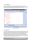
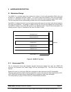
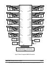
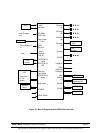
The MARK III consists of four CCAs with growth for two additional CCAs. These CCAs are described in the
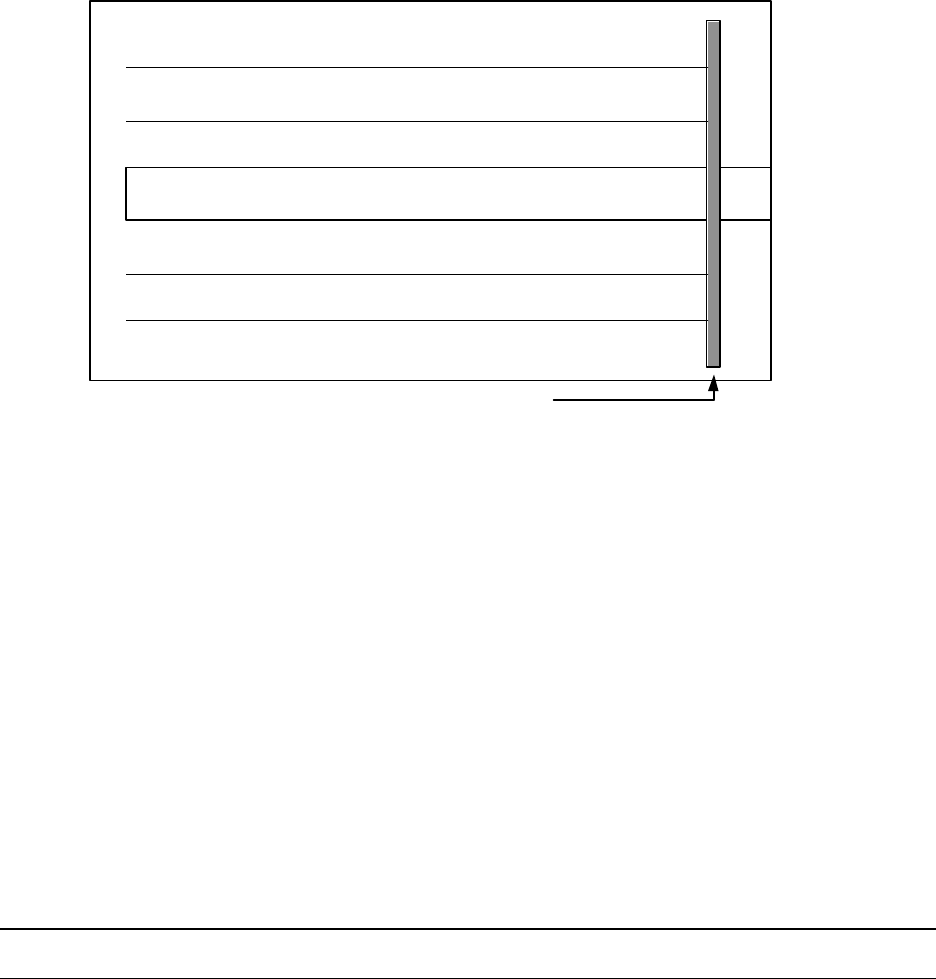
following sections. Figure 31 illustrates the top view of the Mark III CMU.
GROWTH CCA #1
PROCESSOR CCA
INPUT/OUTPUT CCA
GROWTH CCA #2
POWER SUPPLY ARINC 600
INTERCONNECT CCA
Figure 31 MARK III Top View
5.1.1 Interconnect CCA
The A1 Interconnect circuit card assembly provides interconnect between the unit's rear ARINC 600
connector, the Processor CCA, Power Supply CCA and Input/Output CCA. The CCA has the following
features:
Signals are routed in a multi-layer PWB that is designed to reduce emissions and RF Susceptibility.
The circuit card assembly contains lightning suppression circuitry that meets the latest requirements of DO-
160D. ARINC 600 connector pins are replaceable on an individual pin basis (front removable).
The interconnection of plug-in CCAs is done by PCI Bus-Based connectors.