


39
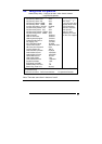
DRAM Timing Selectable
The first chipset settings deal with CPU access to dynamic random
access memory (DRAM). The default timings have been carefully
chosen and should only be altered if data is being lost. Such a scenario
might well occur if the system had mixed speed DRAM chips installed so
that greater delays may be required to preserve the integrity of the data
held in the slower memory chips.
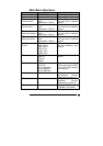
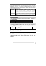
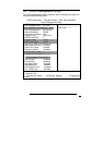
CAS Latency Time
When synchronous DRAM is installed, the number of clock cycles of CAS
latency depends on the DRAM timing.
The Choice: 1.5 , 2, 2.5, 3
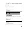
DRAM Cycle Time Tras/Trc
Select the number of SCLKs for an access cycle.
The choice: 5/7, 6/8.
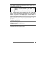
DRAM RAS# to CAS# Delay
z This field lets users insert a timing delay between the CAS and RAS
strobe signals.
z It is used when DRAM is written to, read from, or refreshed.
z Choice 2 means shorter delay which shortens the process of charging;
and choice 3 means longer delay which lengthens the process of
charging.
z This field applies only if the synchronous DRAM is installed in the
system.
The choice: 2, 3.
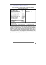
DRAM RAS# Precharge
If an insufficient number of cycles is allowed for the RAS to accumulate
its charge before DRAM refresh, the refresh may be incomplete and the
DRAM may fail to retain data. Fast gives faster performance; and Slow
gives more stable performance. This field applies only when
synchronous DRAM is installed in the system.
The choice: 2, 3.