OVERVIEW OF NUMERIC PROCESSING
80286 memory management and protection mechanisms. The 80286 Processor Extension Data Channel
and the hardware interface between the
80286 and 80287 processors are described
in
Chapter Six of
the
80286 Hardware Reference Manual.
From the programmer's perspective, the
80287 can be considered just an extension of the 80286
processor. All interaction between the 80286 and the 80287 processors
on
the hardware level
is
handled
automatically by the
80286 and
is
transparent to the software. . "
To communicate with the 80287, the 80286 uses the reserved
I/O
port addresses 00F8H,
OOFAH,
and
OOFCH
(I/O
ports numbered 00F8H through
OOFFH
are reserved for the 80286/80287 interface).
These
I/O
operations are performed automatically by the 80286 and are distinct from
I/O
operations
that
result from program
I/O
instructions.
I/O
operations resulting from the execution of ESC instruc-
tions are completely transparent to software. Any program may execute ESCAPE (numeric) instruc-
tions,
without regard to its current
I/O
Privilege Level (IOPL). .
To guarantee correct operation of the
80287, 'programs must not perform any explicit
I/O
operations
to any of the eight ports reserved for the
80287. The
10PL
of the 80286 can be used to protect the
integrity of
80287 computations
in
multiuser reprogrammable applications, preventing any accidental
or other tampering with the
80287 (see Chapter Eight of the 80286 Operating System Writer's Guide).
80287
NUMERIC
PROCESSOR
ARCHITECTURE
To the programmer, the 80287
NPX
appears as a set of additional registers complementing those of
the
80286. These additional registers consist of
• Eight
indi~idually-addressable
80-bit numeric registers, organized as a register stack
• Three sixteen-bit registers containing;
an
NPX
status word
an
NPX
control word
a tag word
• Four 16-bit registers containing the
NPX
instruction and data pointers
All of the
NPX
numeric "instructions focus
on
the contents of these
NPX
registers.
The
NPX
Register Stack
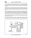
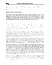
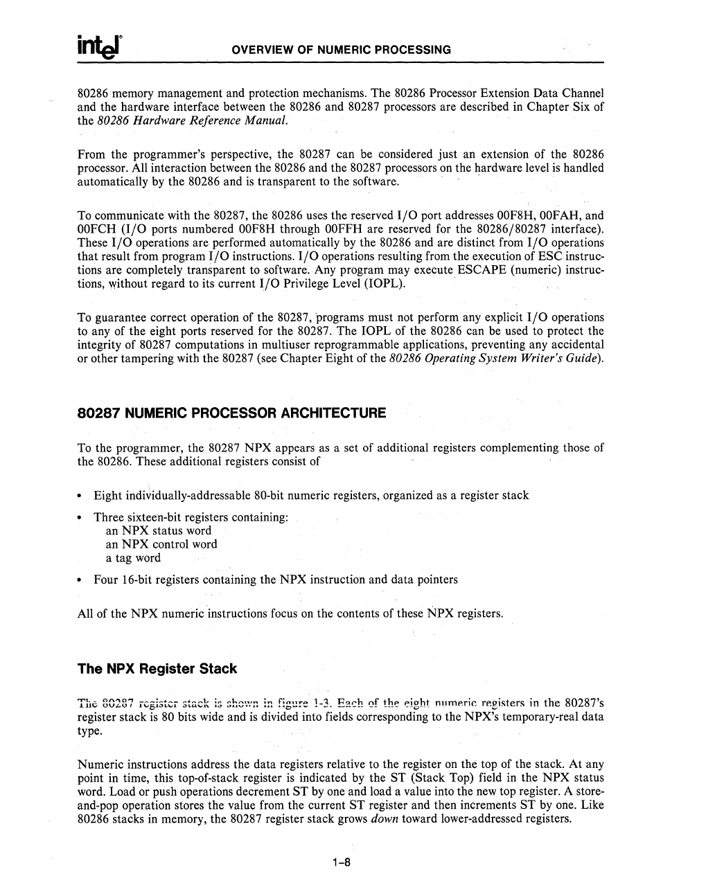
The 80287 register
:;tack
h;
:;hc'.'"/n
in
fig!!re
1-3.
E2.,=h
of
the.
e.ight
~l)mp.ric
registers
in
the 80287's
register stack
is
80 bits wide and
is
divided into fields corresponding to the NPX's temporary-real data
type.
Numeric instructions address the data registers relative to the register
on
the top of the stack. At any
point in time, this top-of-stack register
is
indicated by the ST (Stack Top) field in the
NPX
status
word. Load or push operations decrement
ST
by one and load a value into the
new
top register. A store-
and-pop operation stores the value from the current
ST
register and then increments ST by one. Like
80286 stacks in memory, the 80287 register stack grows down toward lower-addressed registers.
1-8


