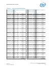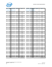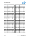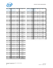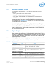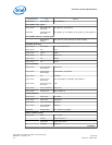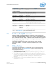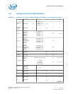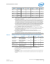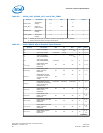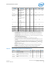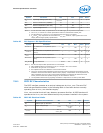
Symbol Parameter Min Typ Max Unit Note
1
P
MAX
2013D PCG
P
MAX
— — 153 W 9
P
MAX
2013C PCG
P
MAX
— — 121 W 9
P
MAX
2013B PCG
P
MAX
— — 99 W 9
P
MAX
2013A PCG
P
MAX
— — 83 W 9
Notes: 1. Unless otherwise noted, all specifications in this table are based on estimates and simulations or
empirical data. These specifications will be updated with characterized data from silicon
measurements at a later date.
2. Each processor is programmed with a maximum valid voltage identification value (VID) that is set
at manufacturing and cannot be altered. Individual maximum VID values are calibrated during
manufacturing such that two processors at the same frequency may have different settings within
the VID range. This differs from the VID employed by the processor during a power management
event (Adaptive Thermal Monitor, Enhanced Intel SpeedStep Technology, or Low Power States).
3. The voltage specification requirements are measured across VCC_SENSE and VSS_SENSE lands at
the socket with a 20-MHz bandwidth oscilloscope, 1.5 pF maximum probe capacitance, and 1-MΩ
minimum impedance. The maximum length of ground wire on the probe should be less than 5
mm. Ensure external noise from the system is not coupled into the oscilloscope probe.
4. I
CC_MAX
specification is based on the V
CC
loadline at worst case (highest) tolerance and ripple.
5. The V
CC
specifications represent static and transient limits.
6. The loadlines specify voltage limits at the die measured at the VCC_SENSE and VSS_SENSE lands.
Voltage regulation feedback for voltage regulator circuits must also be taken from processor
VCC_SENSE and VSS_SENSE lands.
7. PSx refers to the voltage regulator power state as set by the SVID protocol.
8. PCG is Platform Compatibility Guide (previously known as FMB). These guidelines are for
estimation purposes only.
9. P
MAX
is the maximum power the processor will dissipate as measured at VCC_SENSE and
VSS_SENSE lands. The processor may draw this power for up to 10 ms before it regulates to PL2.
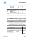
Table 41. Memory Controller (V
DDQ
) Supply DC Voltage and Current Specifications
Symbol Parameter Min Typ Max Unit Note
V
DDQ
(DC+AC)
DDR3/DDR3L
Processor I/O supply
voltage for DDR3/DDR3L
(DC + AC specification)
Typ-5% 1.5 Typ+5% V 2, 3, 5
V
DDQ
(DC+AC)
DDR3/DDR3L
Processor I/O supply
voltage for DDR3L (DC +
AC specification)
Typ-5% 1.35 Typ+5% V 2, 3, 6
Icc
MAX_VDDQ
(DDR3/
DDR3L)
Max Current for V
DDQ
Rail
— — 2.5 A
I
CCAVG_VDDQ (Standby)
Average Current for V
DDQ
Rail during Standby
— 12 20 mA 4
Notes: 1. The current supplied to the DIMM modules is not included in this specification.
2. Includes AC and DC error, where the AC noise is bandwidth limited to under 20 MHz.
3. No requirement on the breakdown of AC versus DC noise.
4. Measured at 50 °C
5. This specification applies to UP Server/Workstation processors paired with a PCH configured with
Intel AMT FW
6. This specification applies to UP Server/workstation processors paired with a PCH configured with
SPS FW
Electrical Specifications—Processor
Intel
®
Xeon
®
Processor E3-1200 v3 Product Family
June 2013 Datasheet – Volume 1 of 2
Order No.: 328907-001 95


