Intel NetStructure
®
MPCBL0010 Single Board Computer
October 2006 Technical Product Specification
Order Number: 304120 161
Telecom Clock—MPCBL0010 SBC
12.0 Telecom Clock
12.1 Functional Description
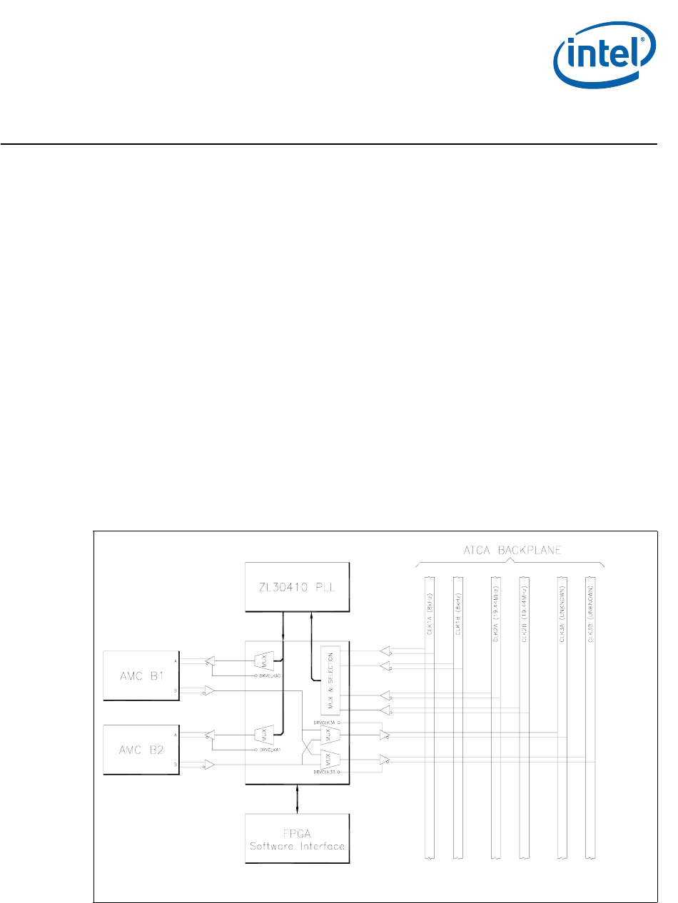
The MPCBL0010 SBC has a built-in telecom clock synchronization circuit. This circuit
uses the Zarlink* ZL30410* Multi-Service Line Card PLL and a PLD that act as a clock
multiplexer on inputs and outputs. The clock can be synchronized to the AdvancedTCA*
backplane clocks, and the output clocks can be routed to the AdvancedMC* CLKA and
CLKB signals.
Control and status registers are implemented in the FPGA. States are synchronized
between the FPGA and the PLD through a 33 MHz full-duplex synchronous serial link.
The FPGA is attached to the main processor as well as the IPMC to allow for flexibility
and simple access to the control/status registers.
The main features of the telecom clock are:
• Redundant reference clock pair selection from CLK1A, 1B with 8 kHz and CLK2A, 2B
with 19.44 MHz
• Automatic hitless switching between selected redundant reference clock pair
(between CLK1A and CLK1B, or CLK2A and CLK2B)
• Provision of line transmission clocks with diverse frequencies to the AdvancedMC
modules
• Setup and alarm interface through the I
2
C bus and additional interrupt signal
Figure 31. Block Diagram of the Telecom Clock


