


Customer Reference Board Manual February, 2005 7
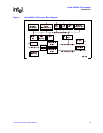
Intel® IQ80333 I/O Processor
Contents
Tables
1Intel
®
80333 I/O Processor Related Documentation List..............................................................9
2 Electronic Information.................................................................................................................10
3 Component Reference................................................................................................................10
4 Terms and Definitions.................................................................................................................11
5 Summary of Features .................................................................................................................14
6 Form-Factor/Connectivity Features ............................................................................................26
7 Power Features ..........................................................................................................................27
8 Flash Memory Requirements......................................................................................................29
9 External Interrupt Routing to Intel
®
80333 I/O Processor...........................................................30
10 Peripheral Bus Features.............................................................................................................31
11 Flash ROM Features ..................................................................................................................32
12 Rotary Switch Requirements ......................................................................................................33
13 Battery Status Buffer Requirements ...........................................................................................34
14 Reset Requirements/Schemes...................................................................................................37
15 Switch Summary.........................................................................................................................38
16 Switch S7A1 ...............................................................................................................................38
17 Jumper Summary .......................................................................................................................39
18 Connector Summary...................................................................................................................39
19 J2D2 GPIO Header Definition.....................................................................................................39
20 Rotary Switch Settings................................................................................................................40
21 S7A1-1: PCI-X Bus A Speed Enable..........................................................................................40
22 Switch S7A1-2: Reset IOP: Settings and Operation Mode.........................................................41
23 Switch S7A1-3: RETRY: Settings and Operation Mode .............................................................41
24 S7A1-4: PCI-X Bus B Speed Enable: Settings and Operation Mode .........................................41
25 S7A1-5: PCI-X Bus B Hot-Plug Reset Disable: Settings and Operation Mode ..........................41
26 Switch S7A1- 6: Hot Plug Capable Disabled: Settings and Operation Mode .............................41
27 Switch S7A1 - 7: SMBUS Manageability Address Bit 0: Settings and Operation Mode .............42
28 Switch S7A1 - 8: SMBUS Manageability Address Bit 3: Settings and Operation Mode .............42
29 Switch S7A1 - 9: SMBUS Manageability Address Bit 2: Settings and Operation Mode .............42
30 Switch S7A1 - 10: SMBUS Slave Address 0: Settings and Operation Mode .............................42
31 Jumper J7D1: Descriptions.........................................................................................................43
32 Jumper J7D1: Settings and Operation Mode..............................................................................43
33 Jumper J1C1: Descriptions.........................................................................................................43
34 Jumper J1C1: Settings and Operation Mode..............................................................................43
35 Jumper J1D2: Descriptions.........................................................................................................43
36 Jumper J1D2: Settings and Operation Mode..............................................................................43
37 Jumper J7B4: Descriptions.........................................................................................................44
38 Jumper J7B4: Settings and Operation Mode..............................................................................44
39 Jumper J9D3: Descriptions.........................................................................................................44
40 Jumper J9D3: Settings and Operation Mode..............................................................................44
41 Peripheral Bus Memory Map ......................................................................................................47
42 Intel
®
IQ80321 Evaluation Platform Board and
Intel
®
IQ80333 I/O Processor Evaluation Platform Board Comparisons ....................................51
43 Related Documents ....................................................................................................................53