


Installation
•
19
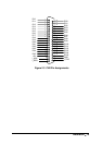
2.7 8254 for Timer Pacer Generation
Timer 0
Timer 1
Timer 2
CLK0
GATE0
OUT0
CLK1
GATE1
CLK2
GATE2
OUT1
OUT2
8254 Timer/Counter
Digital Input Timer Pacer
Digital Output Timer Pacer
4MHz Clock
“H”
“H”
“H”
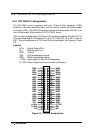
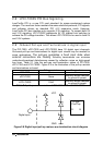
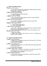
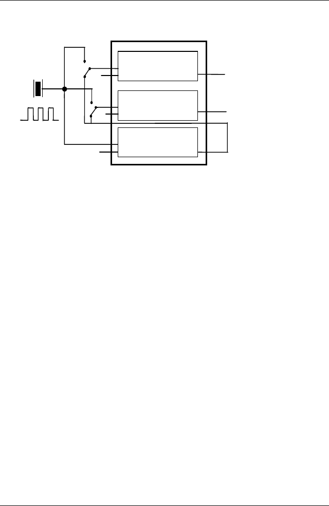
Figure 2.7 8254 configuration
The internal timer/counter 8254 on the PCI-7200 is configured as the above
diagram (Figure 2.7). Users can use it to generate the timer pacer for both
digital input and digital output triggers.
The digital input timer pacer is from OUT0 (Timer 0), and the digital output
timer pacer is from OUT1 (Timer 1). Besides, Timer 0 and Timer 2 can be
cascaded together to generate more timer pacer frequencies for digital input.
Also, Timer 2 can be cascaded with Timer 1 for digital output.
pacer rate = 4MHz / ( C0 * C2)
if Timer 0 & Timer 2 are cascaded
pacer rate = 4MHz / C0
if timer 0 & Timer 2 are not cascaded
The maximum pacer signal rate of input and output are 4MHz/2 = 2Mhz. The
minimum signal rate is 4MHz/65535/65535.
For example, to get a pacer rate of 2.5kHz, set C0 = 40 and C2 = 40. That is
2.5KHz = 4Mhz / (40 x 40)