


H
ARDWARE
R
EFERENCE
G
UIDE
MICRO
-
LINE
C6713CPU
Date : 28 November 2005
Doc. no. : C6713CPU_HRG
Iss./Rev : 1.1
Page : 17
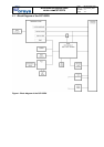
CE0 is used for on-board SDRAM
CE1 is used for on-board flash memory , PLD and FPGA registers.
CE2 and CE3 are used for the FPGA
Please refer to chapter 3 for further descriptions of the CE spaces and their address ranges.
2.5.3 Inter Integrated Circuit (I
2
C) Interfaces
The TMS320C6713 DSP provides two I
2
C interfaces. These 2-wire interfaces can be used for
accessing peripherals, like temperature sensors, EEPROMS, A/D and D/A converters, etc. The I
2
C
interfaces are described in detail in [4] and [9].
At the TMS320C6713 DSP, the signals of I
2
C interface #1 are shared with signals of the McBSP
interface #1. Chapter 6.3 shows the shared signals.
By default, the C6713CPU board only provides the I
2
C interface #1 of the TMS320C6713 DSP. If
the I
2
C interface #0 is also needed for a certain application, a slight hardware reconfiguration of the
C6713CPU board is necessary. In this case please contact ORSYS.
2.5.4 General Purpose Input / Output Pins (GPIO)
At the TMS320C6713 DSP a couple of GPIO pins are shared with the Host Port Interface (HPI).
The HPI is enabled by default, therefore the GPIO signals are not available.
Instead of DSP GPIO pins, a number of other software programmable digital I/O pins can be used:
External flags (XF0, XF1)
Timer signals (TINP0, TINP1 TOUT0, TOUT1)
McBSP signals (see [6], chapter "McBSP Pins as General-Purpose I/O")
Free FPGA pins (requires a BSP or custom FPGA design)
2.5.5 Multi-channel Buffered Serial Ports (McBSP)
The TMS320C6713 DSP provides two independent McBSPs. Each port can communicate a full
duplex, continuous data stream at rates up to 75 Mbps. These ports can be used for inter-
processor communication as well as for connecting industry standard peripheral devices like audio
codecs, A/D or D/A devices etc.
An implemented multi-channel protocol which provides up to 128 channels additionally opens a
variety of applications such as T1/E1 framers, MVIP framers etc.
The McBSPs are compatible to other standard synchronous serial interfaces from Texas
Instrument's TMS320C2000 or ’C5000 DSP families and can be programmed to be compatible
with many other vendors' synchronous serial interfaces. They consist of the signals DRx (data
receive), DXx (data transmit), CLKRx (clock receive), CLKXx (clock transmit), FSRx (frame sync
receive) and FSXx (frame sync transmit). Additionally the TMS320C6713 DSP supports a CLKSx
(clock source) signal. The 'x' in the signal names represent the port number and are 0 or 1 for
McBSP0 or McBSP1 respectively.
The above mentioned signals can also be used as software controllable digital general purpose
inputs or outputs.
Possible general purpose inputs are: DRx, CLKRx, CLKXx, FSRx, FSXx and CLKSx.
Possible general purpose outputs are: DXx, CLKRx, CLKXx, FSRx and FSXx.
On the TMS320C6713 DSP, the McBSP peripherals share signals with
McASP #0
I
2
C #1
On the C6713CPU board, all McBSP signals are routed to micro-line
®
connectors. Chapter 6.3
contains a detailed listing of connector pin assignments as well as a list of shared signals. Detailed
information how to use the McBSPs can be found in [4] and [6].