


H
ARDWARE
R
EFERENCE
G
UIDE
MICRO
-
LINE
C6713CPU
Date : 28 November 2005
Doc. no. : C6713CPU_HRG
Iss./Rev : 1.1
Page : 27
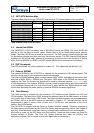
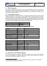
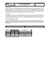
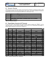
7 6 5 4 3 0
SDA_STAT SDA_CTL SCL_STAT SCL_CTL RESERVED
r, 1 r, w, 1 r, 1 r, w, 1
SDA_STAT:
retrieves the current state of the SDA line. If this bit is read as 1, the SDA line is in a logic high
state and no device pulls the line low. If 0 is read from this bit, the SDA line is pulled low by either
the PLD (SDA_CTL bit), or the temperature sensor.
SDA_CTL:
controls the SDA line. If this bit is set to 0, the SDA line is pulled low by the PLD. If this bit is set to
1, the SDA line is not driven by the PLD. In this case the SDA line may be at logic high level (if the
temperature sensor does not drive this signal, line is then pulled high by a pull-up resistor) or at
logic low level (if the temperature sensor pulls SDA low).
SCL_STAT:
retrieves the current state of the SCL line. Since the PLD is the only clock source of the local I
2
C
bus, it will always reflect the status of the SCL_CTL bit.
SCL_CTL:
controls the SCL line. If this bit is set to 0, the SCL line is pulled low by the PLD. If this bit is set to
1, the SCL line will be released, so it will become high by its pull-up resistor.
3.10.6 External Flag Register (XF)
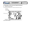
The C6713CPU provides two digital I/O pins, called external flags (XF0, XF1). These I/O pins are
available at the micro-line
®
connectors. They are controllable by the external flag register. Each XF
pin can be programmed to be either an input or an output.
Application software can use the XF pins for any I/O purposes. Examples are:
digital control line for external hardware
digital input for reading the status of external hardware
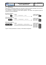
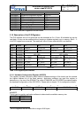
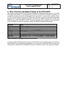
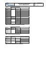
7 6 5 4 3 0
XF1_DIR XF1_DATA XF0_DIR XF0_DATA RESERVED
r, w, 0 r, w r, w, 0 r, w
XF1_DIR controls the direction of the XF1 pin:
If XF1_DIR is set to 1, XF1 is an output. In this case XF1_DATA is read- and writeable. The XF1
pin reflects the status of XF1_DATA (XF1_DATA=1 sets the XF1 pin to +3.3 V).
If XF1_DIR is set to 0, XF1 is an input. In this case XF1_DATA is read-only and reflects the status
of the XF1 pin (XF1 >= 2.0 V: XF1_DATA = 1; XF1 < 0.8 V: XF1_DATA = 0).
XF0_DIR and XF0_DATA have the same functionality, but for the XF0 pin.
Both, the XF1 pin and the XF0 pin are configured as inputs after reset or power-up.
3.10.7 Watchdog Register (WDG)
This register controls operation of the watchdog timer. Application software can enable the
watchdog timer to reset the whole system if the system is no longer working properly.
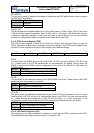
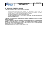
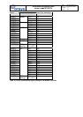
7 6 5 4 3 0
RESERVED WDG_RST WDG_EN RESERVED
r, 00 w, 0 r, w, 0