


H
ARDWARE
R
EFERENCE
G
UIDE
MICRO
-
LINE
C6713CPU
Date : 28 November 2005
Doc. no. : C6713CPU_HRG
Iss./Rev : 1.1
Page : 35
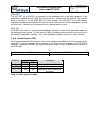
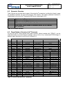
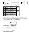
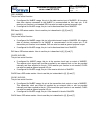
6.4 Pinout of the JTAG Connector
Pin Signal pin signal used for
A1 FPGA_TMS B1 GND
A2 FPGA_TDI B2 GND
A3 FPGA_TDO B3 GND
A4 FPGA_TCK B4 GND
A5 +3.3 V B5 GND
FPGA
A6 not connected B6 not connected unused
A7 CPU_EMU0 B7 CPU_EMU1
A8 CPU_TCK_RET B8 GND
A9 CPU_TCK B9 GND
A10 CPU_TDO B10 GND
A11 +3.3 V B11 not connected
A12 CPU_TDI B12 GND
A13 CPU_TMS B13 /CPU_TRST
DSP
Table 16: Pinout of the JTAG connector
Usually, the JTAG connector is used with an adapter that is part of the development kits. This
adapter provides connectors that are mechanically compatible with the standard development
tools:
JTAG emulators (e.g. XDS510 PP Plus, XDS510 USB, XDS560)
the Xilinx parallel download cable
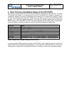
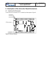
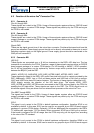
DSP JTAG connec tor
(fits TI emulator POD)
FPGA JTAG connector
A1
B13
B1
A13
TMSTDITDOTCKGND+3.3V
top view
Figure 7: JTAG adapter for the C6713CPU