


H
ARDWARE
R
EFERENCE
G
UIDE
MICRO
-
LINE
C6713CPU
Date : 28 November 2005
Doc. no. : C6713CPU_HRG
Iss./Rev : 1.1
Page : 36
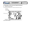
6.5 Function of the micro-line
®
Connector Pins
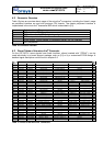
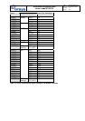
6.5.1 Connector A
Pins A1 through A32:
These signals are routed to the FPGA. Usage of these signals requires either an ORSYS board
support package or a custom FPGA design. These signals are pulled-up by the FPGA as long as
the FPGA is not loaded.
6.5.2 Connector B
Pins B1 through B24:
These signals are routed to the FPGA. Usage of these signals requires either an ORSYS board
support package or a custom FPGA design. These signals are pulled-up by the FPGA as long as
the FPGA is not loaded.
Signal GND:
These are the signal ground pins of the micro-line
®
connector. Peripheral devices should use this
ground as reference. Power supply ground should not be directly connected to these pins to avoid
switching regulator ripple on the signal ground. Power supply ground should be connected to the
GND pins on connector D.
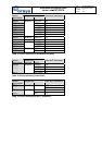
6.5.3 Connector BB
HD[15:0]:
These signals are connected over a 16 bit bus transceiver to the DSP's HPI data bus. The bus
transceiver is controlled by the FPGA. Therefore, usage of these signals requires either an ORSYS
board support package or a custom FPGA design. For HPI booting or McASP / GPIO operation,
the 16 bit bus transceiver can be replaced by resistor arrays which provide direct connections
between the BB[16:1] and the DSP.
HHWIL, HCNTL[1:0], /HAS,HR/W, /HCS, /HRD_HSTRB, /HWR_HSTRB, /HRDY, /HINT:
These signals are routed to the DSP’s HPI control lines and have a pull-up resistor provided by the
DSP. Additionally, /HRDY, has a 4.7k pull-down resistor and /HAS has a 10k pull-up resistor.
/HINT and /HRDY also have 22 series resistors. The function of these signals is described in [6].
HR/W directly controls the direction of the HPI data driver. The signals HR/W, /HCS,
/HRD_HSTRB and /HWR_HSTRB are also connected to the FPGA and are used by the FPGA for
enabling the HPI data driver. These signals are inputs to the DSP. The FPGA should must not
drive these signals if they are driven from an external host processor at the micro-line
®
bus.
Pins BB27 through BB30:
The signals are routed to the FPGA. Usage of these signals requires either an ORSYS board
support package or a custom FPGA design. These signals are pulled-up by the FPGA as long as
the FPGA is not loaded.
SCL0:
This signal is only routed to the FPGA in default hardware configuration, therefore SCL0 is not
available by default. In this case, SCL0 can be used for any purpose by an ORSYS board support
package or a custom FPGA design. Optionally, SCL0 can additionally be connected to the DSP's
I
2
C interface #0, see chapter 7.2.5 for details. When connected, SCL0 has a 10K pull-up resistor.
If the board is configured for I2C #0 usage, then the FPGA may only pull this signal low, according
to the rules of the I
2
C standard.
SDA0:
This signal is only routed to the FPGA in default hardware configuration, therefore SDA0 is not
available by default. In this case, SDA0 can be used for any purpose by an ORSYS board support