


Chapter 4 Arb Operation
DAQArb 5411 User Manual 4-22
©
National Instruments Corporation
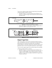
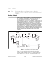
Phase-Locked Loops
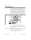
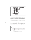
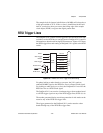
Figure 4-20 illustrates the block diagram for the DAQArb 5411 PLL
circuit. The PLL consists of a voltage controlled crystal oscillator
(VCXO) with a tuning range of ±100 ppm. The main clock of 80 MHz
is generated by this VCXO. The PLL can lock to a reference clock
source from the external connector or a RTSI Osc line on the RTSI bus,
or it can be tuned internally using a calibration DAC (CalDAC). This
tuning has been done at the factory for the best accuracy possible. The
reference clock and the VCXO clock are compared by a phase
comparator running at 1 MHz. The error signal is filtered out by the
loop filter and sent to the control pin of the VCXO to complete the loop.
Figure 4-20.
Phase-Locked Loop (PLL) Architecture
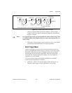
You can phase lock to an external reference clock source of 1 MHz and
from 5–20 MHz in 1 MHz increments. The PLL can lock to a signal
level of at least 1 V
pk-pk
.
Caution: Do not increase the voltage level of the clock signal at the PLL reference
input connector by more than the specified limit, 5 V
pk-pk
.
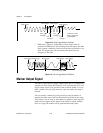
The VCXO output of 80 MHz is further divided by four, to send a
20 MHz board clock signal to the RTSI bus.
80 MHz
Div/4
VCXO
Board Clock (Master)
RTSI Clock (Slave)
Master/Slave
RTSI
Switch
RTSI Bus
RTSI Osc
Board Clock
20 MHz
Loop
Filter
Tune
DAC
PLL Ref
(1 V
pk-pk
min)
Control
Voltage
(20 MHz)
Source
14
Phase
Comp
AMUX
!