Functional Modes of Operation (Continued)
Security Level 2
This security level prevents programming of the on-chip
EPROM or the ECON registers thereby providing WRITE
protection Read accesses to the on-chip EPROM or ECON
registers may be accomplished without constraint in
EPROM Read accesses to the on-chip EPROM may be
accomplished without constraint in NORMAL RUNNING
mode
Security Level 1
This security level prevents programming of the on-chip
EPROM or ECON registersthereby providing registers
write protection Read accesses to the on-chip ECON-regis-
ters may be accomplished without constraint in EPROM
mode Read accesses to the on-chip EPROM will produce
ENCRYPTED data in EPROM READ accesses to the on-
chip EPROM during NORMAL RUNNING mode are sub-
ject to Runtime Memory Protection Under Runtime Mem-
ory Protection only instruction opcodes stored within the
on-chip EPROM are allowed to access the EPROM as oper-
and If any other instruction opcode attempts to use the
contents of EPROM as an operand it will receive the hex
value ‘‘FF’’ The Runtime Memory Protection feature is de-
signed to prevent hostile software running from external
memory or on-chip RAM from reading secured EPROM
data Transfers of control into or out of the on-chip EPROM
(such as jump or branch) are not affected by Runtime Mem-
ory Protection Interrupt vector fetches from EPROM pro-
ceed normally and are not affected by Runtime Memory
Protection
Security Level 0
This security level prevents programming of the on-chip
EPROM or ECON registers thereby providing write protec-
tion Read accesses to the on-chip ECON registers may be
accomplished without constraint in EPROM mode READ
accesses to the on-chip EPROM are NOT ALLOWED in
EPROM mode Such accesses will return data value ‘‘FF’’
hex Runtime Memory Protection is enforced as in security
level 1
These four levels of security help ensure that the user
EPROM code is not tampered with in a test fixture and that
code executing from RAM or external memory does not
dump the user algorithm
Erasure Characteristics
The erasure characteristics of the HPC167064 are such that
erasure begins to occur when exposed to light with wave-
lengths shorter than approximately 4000 Angstroms () It
should be noted that sunlight and certain types of fluores-
cent lamps have wavelengths in the 3000–4000 range
After programming opaque labels should be placed over
the HPC167064’s window to prevent unintentional erasure
Covering the window will also prevent temporary functional
failure due to the generation of photo currents
The recommended erasure procedure for the HPC167064 is
exposure to short wave ultraviolet light which has a wave-
length of 2537 Angstroms () The integrated dose (ie UV
intensity
c
exposure time) for erasure should be a minimum
of 30W-seccm
2
The HPC167064 should be placed within 1 inch of the lamp
tubes during erasure Some lamps have a filter on their
tubes which should be removed before erasure The era-
sure time table shows the minimum HPC167064 erasure
time for various light intensities
An erasure system should be calibrated periodically The
distance from lamp to unit should be maintained at one inch
The erasure time increases as the square of the distance (If
distance is doubled the erasure time increases by a factor of
4) Lamps lose intensity as they age When a lamp is
changed the distance has changed or the lamp has aged
the system should be checked to make certain full erasure
is occurring
Incomplete erasure will cause symptoms that can be mis-
leading Programmers components and even system de-
signs have been erroneously suspected when incomplete
erasure was the problem
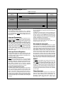
Minimum HPC167064 Erasure Time
Light Intensity Erasure Time
(Micro-Wattscm
2
) (Minutes)
15000 36
10000 50
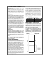
Memory Map of the HPC167064
The HPC167064 has 256 bytes of on-chip user RAM and
chip registers located at address 0000–01FF that is always
enabled and 256 bytes of on-chip RAM located at 0200–
02FF that can be enabled or disabled It has 8 kbytes of on-
chip EPROM located at address 0E000–0FFFF that is al-
ways enabled and 8 kbytes of EPROM located at address
0C000–0DFFF that can be enabled or disabled
The ECON6 contains two bits ROM0 and RAM0 When
these bits are ‘‘1’’ (erased default) full 16 kbytes of ROM
and 512 bytes of RAM are enabled Programming a ‘‘0’’ to
these bits disables the lower 8k for the EPROM and upper
256 bytes for the RAM The ECON registers are only acces-
sible to the user during EPROM mode
Address In Address In Other
EPROM Mode HPC Modes
7FFF Operation
4000 FFFF
3FFF
2000 E000
1FFF DFFF
Enabled or
Disabled by
config logic
0000 C000
–
11


