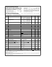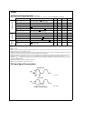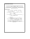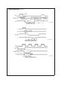
Absolute Maximum Ratings
If MilitaryAerospace specified devices are required
please contact the National Semiconductor Sales
OfficeDistributors for availability and specifications
Total Allowable Source or Sink Current 100 mA
Storage Temperature Range
b
65
Cto
a
150
C
Lead Temperature (Soldering 10 sec) 300
C
V
CC
with Respect to GND
b
05V to 70V
All Other Pins (V
CC
a
05V) to (GND
b
05V)
Note
Absolute maximum ratings indicate limits beyond
which damage to the device may occur DC and AC electri-
cal specifications are not ensured when operating the de-
vice at absolute maximum ratings
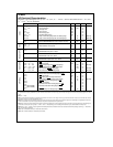
DC Electrical Characteristics
V
CC
e
50V
g
5% unless otherwise specified T
A
eb
55
Cto
a
125
C for HPC167064 and V
CC
e
50V
g
10% unless
otherwise specified T
A
e
0
Cto70
C for HPC467064
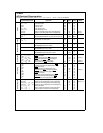
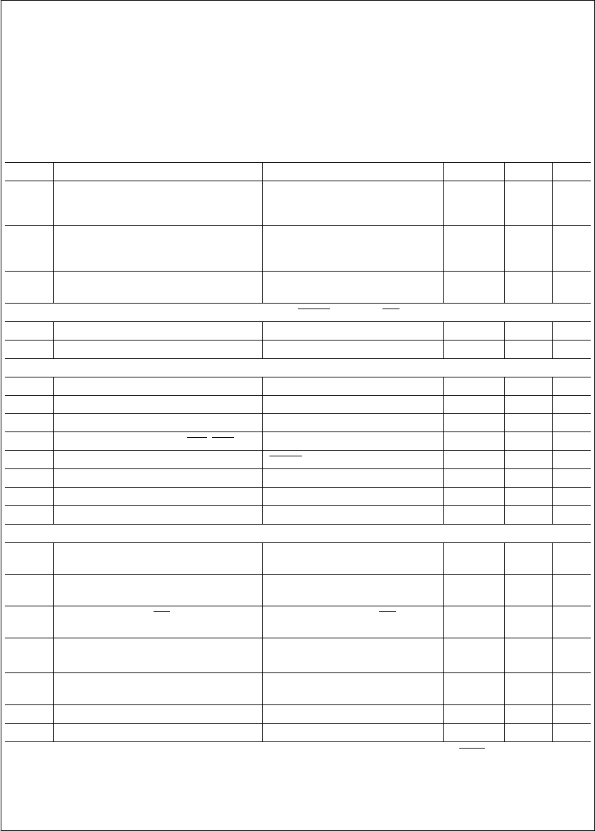
Symbol Parameter Test Conditions Min Max Units
I
CC
1
Supply Current V
CC
e
max f
IN
e
300 MHz (Note 1) 85 mA
V
CC
e
max f
IN
e
200 MHz (Note 1) 70 mA
V
CC
e
max f
IN
e
20 MHz (Note 1) 40 mA
I
CC
2
IDLE Mode Current V
CC
e
max f
IN
e
300 MHz (Note 1) 60 mA
V
CC
e
max f
IN
e
200 MHz (Note 1) 45 mA
V
CC
e
max f
IN
e
20 MHz (Note 1) 1 mA
I
CC
3
HALT Mode Current V
CC
e
max f
IN
e
0 kHz (Note 1) 400 mA
V
CC
e
25V f
IN
e
0 kHz (Note 1) 100 mA
INPUT VOLTAGE LEVELS FOR SCHMITT TRIGGERED INPUTS RESET NMI AND WO AND ALSO CKI
V
IH1 Logic High 09 V
CC
V
V
IL1 Logic Low 01 V
CC
V
ALL OTHER INPUTS
V
IH2
Logic High 07 V
CC
V
V
IL2
Logic Low 02 V
CC
V
I
LI1
Input Leakage Current V
IN
e
0 and V
IN
e
V
CC
(Note 4)
g
2 mA
I
LI2
Input Leakage Current RDYHLD EXUI V
IN
e
0
b
3
b
50 mA
I
LI3
Input Leakage Current B12 RESET
e
0 V
IN
e
V
CC
05 7 mA
I
LI4
Input Leakage Current EXM V
IN
e
0 and V
IN
e
V
CC
(Note 4)
g
10 mA
C
I
Input Capacitance (Note 2) 10 pF
C
IO
IO Capacitance (Note 2) 20 pF
OUTPUT VOLTAGE LEVELS
V
OH1
Logic High (CMOS) I
OH
eb
10 mA (Note 2) V
CC
b
01
01 V
V
OL1
Logic Low (CMOS) I
OH
e
10 mA (Note 2)
V
OH2
Port AB Drive CK2 I
OH
eb
7 mA 24
04 V
V
OL2
(A0–A15 B10 B11 B12 B15) I
OL
e
3mA
V
OH3
Other Port Pin Drive WO (open drain) I
OH
eb
16 mA (except WO) 24
04 V
V
OL3
(B0–B9 B13 B14 P0–P3) I
OL
e
05 mA
V
OH4
ST1 and ST2 Drive I
OH
eb
6 mA 24
04 V
V
OL4
I
OL
e
16 mA
V
OH5
Port AB Drive (A0–15 B10 B11 B12 B15) I
OH
eb
1 mA 24
04 V
V
OL5
when used as External AddressData Bus I
OL
e
3mA
V
RAM
RAM Keep-Alive Voltage (Note 3) 25 V
CC
V
I
OZ
TRI-STATE
Leakage Current V
IN
e
0 and V
IN
e
V
CC
g
5 mA
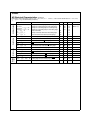
Note 1I
CC
1
I
CC
2
I
CC
3
measured withno external drive (I
OH
and I
OL
e
0 I
IH
I
IL
e
0 andEXM
e
V
CC
) I
CC1
is measuredwith RESET
e
GND I
CC3
is measured
with NMI
e
V
CC
CKI driven to V
IH1
and V
IL1
with rise and fall times less than 10 ns
Note 2 This is guaranteed by design and not tested
Note 3 Test duration is 100 ms
Note 4The EPROM modeof operationfor thisdevice requires highvoltage inputon pins EXMV
PP
I3I4 I5 I6and I7This willincrease the inputleakage current
above the normal specification when driven to voltages greater than V
CC
a
03V
See NORMAL RUNNING MODE
2


