


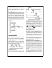
Universal Peripheral Interface
The Universal Peripheral Interface (UPI) allows the
HPC167064 to be used as an intelligent peripheral to anoth-
er processor The UPI could thus be used to tightly link two
HPC167064’s and set up systems with very high data ex-
change rates Another area of application could be where a
HPC167064 is programmed as an intelligent peripheral to a
host system such as the Series 32000
microprocessor
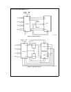
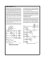
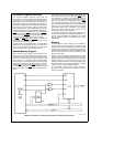
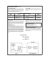
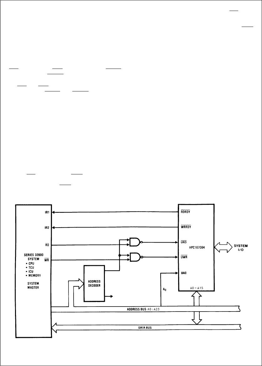
Figure 27
illustrates how a HPC167064 could be used as an
intelligent peripheral for a Series 32000-based application
The interface consists of a Data Bus (port A) a Read Strobe
(URD
) a Write Strobe (UWR) a Read Ready Line (RDRDY)
a Write Ready Line (WRRDY
) and one Address Input (UA0)
The data bus can be either eight or sixteen bits wide
The URD
and UWR inputs may be used to interrupt the
HPC167064 The RDRDY
and WRRDY outputs may be
used to interrupt the host processor
The UPI contains an Input Buffer (IBUF) an Output Buffer
(OBUF) and a Control Register (UPIC) In the UPI mode
Port A on the HPC167064 is the data bus UPI can only be
used if the HPC167064 is in the Single-Chip mode
Shared Memory Support
Shared memory access provides a rapid technique to ex-
change data It is effective when data is moved from a pe-
ripheral to memory or when data is moved between blocks
of memory A related area where shared memory access
proves effective is in multiprocessing applications where
two CPUs share a common memory block The HPC167064
supports shared memory access with two pins The pins are
the RDYHLD
input pin and the HLDA output pin The user
can software select either the Hold or Ready function by the
state of a control bit The HLDA
output is multiplexed onto
Port B
The host uses DMA to interface with the HPC167064 The
host initiates a data transfer by activating the HLD
input of
the HPC167064 In response the HPC167064 places its
system bus in a TRI-STATE Mode freeing it for use by the
host The host waits for the acknowledge signal (HLDA
)
from the HPC167064 indicating that the sytem bus is free
On receiving the acknowledge the host can rapidly transfer
data into or out of the shared memory by using a conven-
tional DMA controller Upon completion of the message
transfer the host removes the HOLD request and the
HPC167064 resumes normal operations
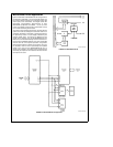
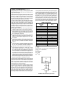
To insure proper operation the interface logic shown is rec-
ommended as the means for enabling and disabling the us-
er’s bus
Figure 28
illustrates an application of the shared
memory interface between the HPC167064 and a Series
32000 system
Memory
The HPC167064 has been designed to offer flexibility in
memory usage A total address space of 64 kbytes can be
addressed with 8 kbytes of EPROM and 512 bytes of RAM
available on the chip itself The EPROM may contain pro-
gram instructions constants or data The EPROM and RAM
share the same address space allowing instructions to be
executed out of RAM
Program memory addressing is accomplished by the 16-bit
program counter on a byte basis Memory can be addressed
directly by instructions or indirectly through the B X and SP
registers Memory can be addressed as words or bytes
Words are always addressed on even-byte boundaries The
HPC167064 uses memory-mapped organization to support
registers IO and on-chip peripheral functions
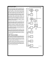
The HPC167064 memory address space extends to
64 kbytes and registers and IO are mapped as shown in
Table III and Table IV
TLDD11046–35
FIGURE 27 HPC167064 as a Peripheral (UPI Interface to Series 32000 Application)
24