


30 MHz
AC Electrical Characteristics
(Continued)
(See Notes 1 and 4 and
Figures 1
thru
5
) V
CC
e
5V
g
10% T
A
e
0
Cto
a
70
C for HPC467064 (Continued)
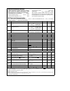
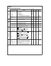
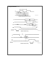
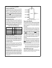
Symbol and Formula Parameter Min Max Units Notes
t
ARR
e
t
C
b
5 ALE Falling Edge to RD Falling Edge 12 ns
t
ACC
e
t
C
a
WS
b
32 Data Input Valid after Address Output Valid 100 ns
t
RD
e
t
C
a
WS
b
39 Data Input Valid after RD Falling Edge 60 ns
t
RW
e
t
C
a
WS
b
14 RD Pulse Width 85 ns
t
DR
e
t
C
b
15 Hold of Data Input Valid after RD Rising Edge 0 35 ns
t
RDA
e
t
C
b
15 Bus Enable after RD Rising Edge 51 ns
t
ARW
e
t
C
b
5 ALE Falling Edge to WR Falling Edge 28 ns
t
WW
e
t
C
a
WS
b
15 WR Pulse Width 101 ns
t
V
e
t
C
a
WS
b
5 Data Output Valid before WR Rising Edge 94 ns
t
HW
e
t
C
b
10 Hold of Data Valid after WR Rising Edge 7 ns
t
DAR
e
t
C
a
WS
b
50 Falling Edge of ALE to Falling Edge of RDY 33 ns
t
RWR
e
t
C
RDY Pulse Width 66 ns
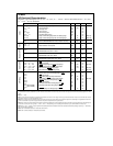
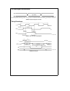
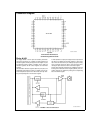
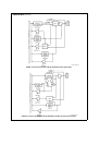
Read CyclesWrite Cycles
Ready
Input
This maximum frequencyis attainable provided that thisexternal baud clock hasa duty cycle such thatthe high period includestwo (2) falling edges ofthe CK2
clock
Note C
L
e
40 pF
Note 1 These AC Characteristicsare guaranteed with external clock drive onCKI having 50% duty cycle and withless than 15 pF load on CKOwith rise and fall
times (t
CKIR
and t
CKIL
) on CKI input less than 25 ns
Note 2 Donot design withthis parameter unlessCKI is drivenwith an active signalWhen using apassive crystal circuitits stability isnot guaranteed if eitherCKI
or CKO is connected to any external logic other than the passive components of the crystal circuit
Note 3t
HAE
is spec’dfor casewith HLD fallingedge occurringat thelatest timecan be acceptedduring thepresent CPUcycle beingexecuted If HLDfalling edge
occurs later t
HAE
may be as long as (3t
C
a
4WS
a
72t
C
a
100) depending on the following CPU instruction cycles its wait states and ready input
Note 4WS
e
t
WAIT
c
(number ofpre-programmed wait states)Minimum andmaximum values arecalculated atmaximum operating frequencyt
c
e
3000 MHz
with one wait state programmed
Note 5 Due to emulation restrictionsactual limits will be better
Note 6 Due to tester limitationsactual limits will be better
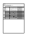
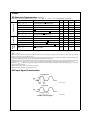
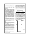
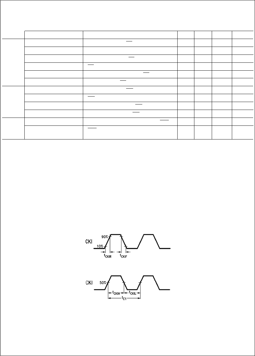
CKI Input Signal Characteristics
RiseFall Time
TLDD11046–2
Duty Cycle
TLDD11046–3
FIGURE 1 CKI Input Signal
6