Timer Overview (Continued)
Maximum output frequency for any timer output can be ob-
tained by setting timerregister pair to zero This then will
produce an output frequency equal to the frequency of
the source used for clocking the timer
Timer Registers
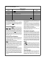
There are four control registers that program the timers The
divide by (DIVBY) register programs the clock input to tim-
ers T2 and T3 The timer mode register (TMMODE) contains
control bits to start and stop timers T1 through T3 It also
contains bits to latch acknowledge and enable interrupts
from timers T0 through T3 The control register PWMODE
similarly programs the pulse width timers T4 through T7 by
allowing them to be started stopped and to latch and en-
able interrupts on underflows The PORTP register contains
bits to preset the outputs and enable the synchronous timer
output functions
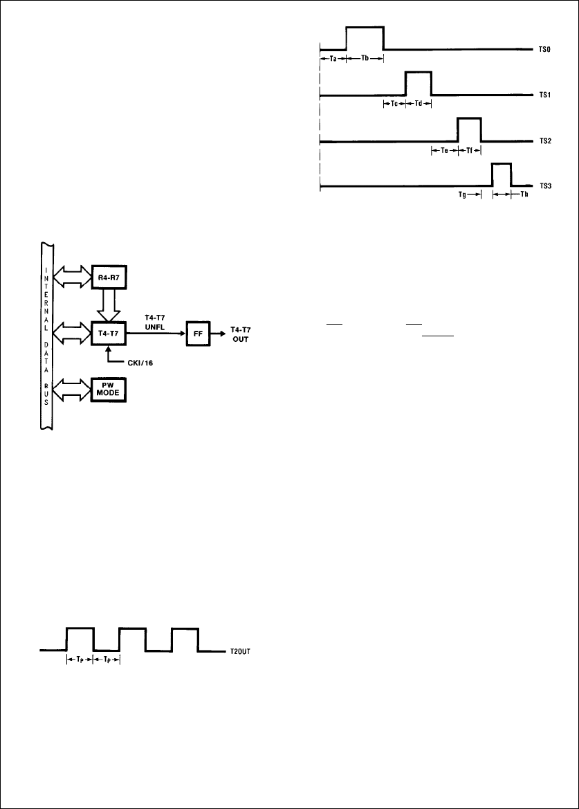
TLDD11046–29
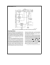
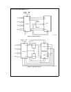
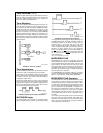
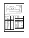
FIGURE 21 Timers T4–T7 Block
Timer Applications
The use of Pulse Width Timers for the generation of various
waveforms is easily accomplished by the HPC167064
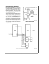
Frequencies can be generated by using the timerregister
pairs A square wave is generated when the register value is
a constant The duty cycle can be controlled simply by
changing the register value
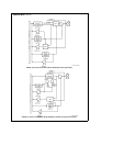
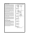
Synchronous outputs based on Timer T2 can be generated
on the 4 outputs TS0–TS3 Each output can be individually
programmed to toggle on T2 underflow Register R2 con-
tains the time delay between events
Figure 23
is an exam-
ple of synchronous pulse train generation
TLDD11046–31
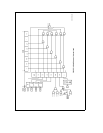
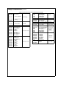
FIGURE 22 Square Wave Frequency Generation
WATCHDOG Logic
The WATCHDOG Logic monitors the operations taking
place and signals upon the occurrence of any illegal activity
TLDD11046–30
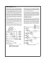
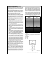
FIGURE 23 Synchronous Pulse Generation
The illegal conditions that trigger the WATCHDOG logic are
potentially infinite loops and illegal addresses Should the
WATCHDOG register not be written to before Timer T0
overflows twice or more often than once every 4096
counts an infinite loop condition is assumed to have oc-
curred An illegal condition also occurs when the processor
generates an illegal address when in the Single-Chip
modes Any illegal condition forces the WATCHDOG Out-
put (WO
) pin low The WO pin is an open drain output and
can be connected to the RESET
or NMI inputs or to the
users external logic
Note See Operating Modes for details
MICROWIREPLUS
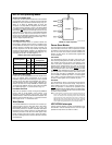
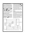
MICROWIREPLUS is used for synchronous serial data
communications (see
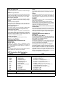
Figure 24
) MICROWIREPLUS has
an 8-bit parallel-loaded serial shift register using SI as the
input and SO as the output SK is the clock for the serial
shift register (SIO) The SK clock signal can be provided by
an internal or external source The internal clock rate is pro-
grammable by the DIVBY register A DONE flag indicates
when the data shift is completed
The MICROWIREPLUS capability enables it to interface
with any of National Semiconductor’s MICROWIRE periph-
erals (ie AD converters display drivers EEPROMs)
MICROWIREPLUS Operation
The HPC167064 can enter the MICROWIREPLUS mode
as the master or a slave A control bit in the IRCD register
determines whether the HPC167064 is the master or slave
The shift clock is generated when the HPC167064 is config-
ured as a master An externally generated shift clock on the
SK pin is used when the HPC167064 is configured as a
slave When the HPC167064 is a master the DIVBY regis-
ter programs the frequency of the SK clock The DIVBY
register allows the SK clock frequency to be programmed in
15 selectable steps from 64 Hz to 1 MHz with CKI at
160 MHz
The contents of the SIO register may be accessed through
any of the memory access instructions Data waiting to be
transmitted in the SIO register is clocked out on the falling
edge of the SK clock Serial data on the SI pin is clocked in
on the rising edge of the SK clock
21


