


Chapter 2 Hardware Overview
NI PCI-1410 User Manual 2-2 ni.com
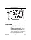
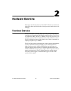
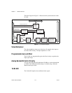
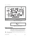
The block diagram in Figure 2-1 illustrates the key functional units of the
NI 1410.
Figure 2-1. NI 1410 Block Diagram
Video Multiplexer
The video multiplexer routes one of the four AC-coupled video inputs to
the 10-bit ADC circuitry. The input impedance is 75 Ω.
Programmable Gain and Offset
The NI 1410 uses programmable gain and offset circuitry to optimize the
input signal range.
Analog Bandwidth Control Circuitry
You can select either the full bandwidth of 30 MHz or a reduced bandwidth
of 9 MHz. The 9 MHz bandwidth setting is available using a 5th order
Butterworth lowpass filter.
10-Bit ADC
The 10-bit ADC digitizes the conditioned video signal.
Digital
Input/Output
Circuitry
RTSI Bus
68-pin VHDCI Connector
Video 0
PCI Bus
Video
Mux
Programmable
Gain and Offset
PCI Interface and
Scatter-Gather
DMA Controller
Onboard
Memory and
Control Circuitry
Analog
Bandwidth
Control
Circuitry
10-Bit
ADC
Digital
Filter
and
LUT
BNC
Video
0,1,2,3
Acquisition and
Region-of-Interest
Control
Genlock Circuit
and SYNC Mux
Aspect Ratio Correction
HSYNC, VSYNC
PCLK
External PCLK,
HSYNC, VSYNC
External CSYNC
4 Camera Control Lines
4 External Triggers