


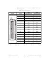
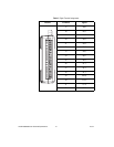
© National Instruments Corporation 21 NI USB-6008/6009 User Guide and Specifications
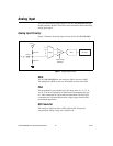
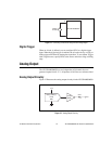
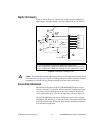
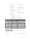
Digital I/O Circuitry
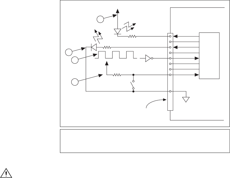
Figure 14 shows P0.<0..7> connected to example signals configured as
digital inputs and digital outputs. You can configure P1.<0..3> similarly.
Figure 14. Example of Connecting a Load
Caution
Exceeding the maximum input voltage ratings or maximum output ratings, which
are listed in the Specifications section, can damage the device and the computer. National
Instruments is not liable for any damage resulting from such signal connections.
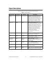
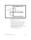
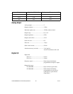
Source/Sink Information
The default configuration of the NI USB-6008/6009 DIO ports is open
collector, allowing 5 V operation, with an onboard 4.7 kΩ pull-up resistor.
An external user-provided pull-up resistor can be added to increase the
source current drive up to a 8.5 mA limit per line as shown in Figure 15.
The NI USB-6009 ports can also be configured as active drive using the
NI-DAQmx API, allowing 3.3 V operation with a source/sink current limit
of ±8.5 mA. Refer to the NI-DAQmx Help for more information about how
to set the DIO configuration.
1 P0.0 configured as an open collector digital output driving an LED
2 P0.2 configured as an active drive digital output driving an LED
3 P0.4 configured as a digital input receiving a TTL signal from a gated invertor
4 P0.7 configured as a digital input receiving a 0 V or 5 V signal from a switch
+5 V
LED
Switch
I/O Connector
GND
P0.0
P0.1
P0.2
P0.3
P0.4
P0.5
P0.6
P0.7
+5 V
LED
1
2
3
4
TTL Signal