


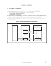

CHAPTER 2 NAMES AND FUNCTIONS OF COMPONENTS
User’s Manual U14337EJ1V0UM00
20
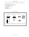
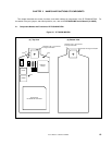
(1)
TEST pins (TP5, TP11, TP12)
These are pins used for testing the analog signals of the standalone emulator.
•
TP 5: GND
•
TP 11: GND
•
TP 12: GND
(2) JP1
This is a pin board for product check. Mount nothing on JP1.
(3) JP2, JP4
These are pin boards for product check. Use and retain the factory settings (pins 2 and 3 shorted) (For details,
refer to
2.2 Clock Settings
)
(4) JP3
This is a pin board for supplying the subsystem clock. (For details, refer to
2.2 Clock Settings
)
(5) JP5
This is a jumper for switching the main system clock supply source.
(6) JP6
This is a pin board for product check. Use and retain the factory settings (pins 1 and 2 shorted).
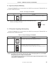
(7) LED
LED for V
PP
ON: Voltage is applied to V
PP
OFF: Voltage is not applied to V
PP
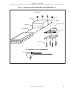
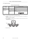
(8) Connector for IE-703002-MC connection
This is a connector for connecting with the IE-703002-MC.
(9) Connector for target connection
This is a connector for connecting with the target system or the extension probe.